semi合集-English.pdf - 第6175页
SEMI G37-88 © SEMI 198 6, 1988 4 Figure 4 Package Warpage Warp in m i ls/Length in Inches = Warp Factor Figure 5 Shoulder Bend Location Figure 6 Lead Co-plan arity NOTICE: T hese st andards do not purport to address s af…
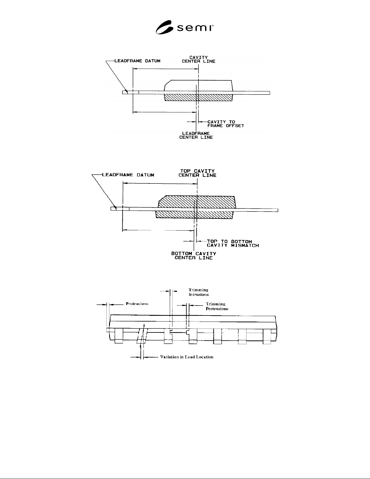
SEMI G37-88 © SEMI 1986, 19883
Figure 1
Cavity to Frame Offset
Figure 2
Cavity Mismatch
Figure 3
Parting Line Protrusions
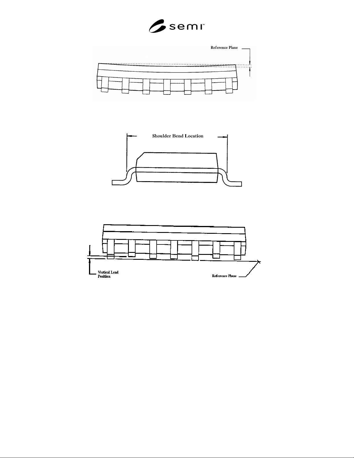
SEMI G37-88 © SEMI 1986, 1988 4
Figure 4
Package Warpage Warp in mils/Length in Inches = Warp Factor
Figure 5
Shoulder Bend Location
Figure 6
Lead Co-planarity
NOTICE: These standards do not purport to address safety issues, if any, associated with their use. It is the
responsibility of the user of these standards to establish appropriate safety and health practices and determine the
applicability of regulatory limitations prior to use. SEMI makes no warranties or representations as to the suitability
of the standards set forth herein for any particular application. The determination of the suitability of the standard is
solely the responsibility of the user. Users are cautioned to refer to manufacturer’s instructions, product labels,
product data sheets, and other relevant literature respecting any materials mentioned herein. These standards are
subject to change without notice.
The user’s attention is called to the possibility that compliance with this standard may require use of copyrighted
material or of an invention covered by patent rights. By publication of this standard, SEMI takes no position
respecting the validity of any patent rights or copyrights asserted in connection with any item mentioned in this
standard. Users of this standard are expressly advised that determination of any such patent rights or copyrights and
the risk of infringement of such rights, are entirely their own responsibility.
Copyright by SEMI® (Semiconductor Equipment and Materials
International), 3081 Zanker Road, San Jose, CA 95134. Reproduction o
f
the contents in whole or in part is forbidden without express written
consent of SEMI.

SEMI G38-0996 © SEMI 1987, 2004 1
SEMI G38-0996 (Reapproved 1104)
TEST METHOD FOR STILL- AND FORCED-AIR JUNCTION-TO-
AMBIENT THERMAL RESISTANCE MEASUREMENTS OF
INTEGRATED CIRCUIT PACKAGES
This test method was technically reapproved by the Global Assembly and Packaging Committee and is the
direct responsibility of the Japanese Packaging Committee. Current edition approved by the Japanese
Regional Standards Committee on July 23, 2004. Initially available at www.semi.org September 2004; to be
published November. Originally published in 1987; previously published September 1996.
1 Purpose
1.1 The purpose of this test is to determine the thermal
resistance of integrated circuit packages using thermal
test chips.
2 Scope
2.1 This test method deals only with junction-to-
ambient measurements of thermal resistance and limits
itself to still- and forced-air convection testing
environments.
NOTICE: This standard does not purport to address
safety issues, if any, associated with its use. It is the
responsibility of the users of this standard to establish
appropriate safety and health practices and determine
the applicability of regulatory or other limitations prior
to use.
3 Referenced Standards
3.1 SEMI Standards
SEMI G32 — Guideline for Unencapsulated Thermal
Test Chip
SEMI G42 — Specification for Thermal Test Board
Standardization for Measuring Junction-to-Ambient
Thermal Resistance of Semiconductor Packages
NOTICE: Unless otherwise indicated, all documents
cited shall be the latest published versions.
4 Terminology
4.1 Definitions
4.1.1 The following definitions and symbols shall
apply for the purpose of this test:
4.1.2 ambient temperature (T
A
, in degrees Celsius) —
the ambient temperature is the temperature of the air at
a specified location in the vicinity of the
microelectronic device under test (DUT).
4.1.3 junction temperature (T
J
, in degrees Celsius) —
the term is used to denote the temperature of the
semiconductor junction in the microcircuit in which the
major part of the heat is generated. For purposes of this
test, the measured junction temperature is only
indicative of the temperature in the immediate vicinity
of the element used to sense the temperature.
4.1.4 power dissipation (P
H
, in watts) — the heating
power applied to the device causing a junction-to-
reference point temperature difference.
4.1.5 temperature-sensitive parameter (TSP) — the
temperature-dependent electrical characteristic of the
junction under test which can be calibrated with respect
to temperature and subsequently used to detect the
junction temperature of interest.
4.1.6 thermal resistance — junction to specified
reference point, R
θJR
degrees Celsius/watt. The thermal
resistance of the microcircuit is the temperature
difference from the junction to some reference point in
the ambient divided by the power dissipation P
H
.
4.1.7 velocity (v
A
, in linear feet per minute (LFPM)) —
the velocity of the air at a specified location upstream
of the DUT.
5 Apparatus
5.1 The apparatus required for these tests shall include
the following as applicable to the specified test
procedures.
5.1.1 Thermocouple Material — Shall be copper
constantan (type T) or equivalent, for the temperature
range −100 to + 300°C. The wire size shall be no larger
than AWG size 30. The junction of the thermocouple
shall be welded to form a bead rather than soldered or
twisted. The accuracy of the thermocouple and
associated measuring system shall be ± 0.5°C.
5.1.2 Suitable Electrical Equipment — As required to
provide controlled levels of conditioning power and to
make the specified measurements. The instrument used
to electrically measure the temperature-sensitive
parameter shall be capable of resolving a voltage
change of 0.5 mV.
5.1.3 Controlled Temperature Chamber, Fluid Bath, or
Wind Tunnel — Capable of maintaining the specific
reference point temperature to within ± 0.5°C of the
reset (measured) value. Typical still-air enclosure and