semi合集-English.pdf - 第933页
SEMI E119-1104 © SEMI 2002, 2004 5 horizontal d atum plane z 8 =35 z 6 28.5 z 12 = 6.25 z 15 4.6 facial datu m plane front side of t he FOBIT where w afers are acce ssed y 5 120 Figure 2 Side View of FOBIT Internal…
SEMI E119-1104 © SEMI 2002, 2004 4
5.5 Wafer Orientation and Numbering — The wafers
must be horizontal when the FOBIT is placed on the
kinematic coupling, and the wafers slots are numbered
in increasing order from bottom to top (so the bottom
wafer is wafer number 1, the next wafer up is wafer
number 2, etc.).
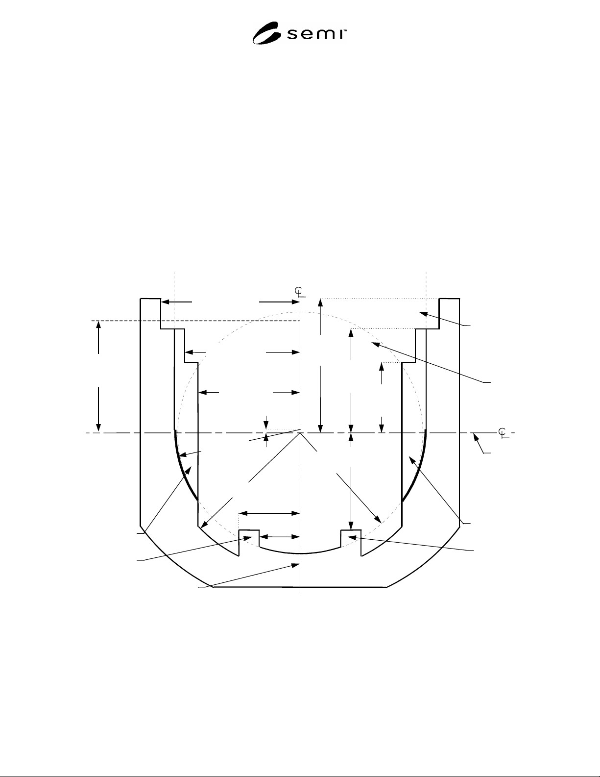
5.6 Internal Horizontal Dimensions — Figure 1 shows
a cross-section of the horizontal boundaries of the
FOBIT side domains (which contain the parts of the
FOBIT higher than z6 above the horizontal datum plane
and lower than z15 above the top wafer). In this and
following figures, the heaviest lines are used for
surfaces that have tolerances (not surfaces that have
only maximum or minimum dimensions). Table 1
defines the dimensions shown in this figure.
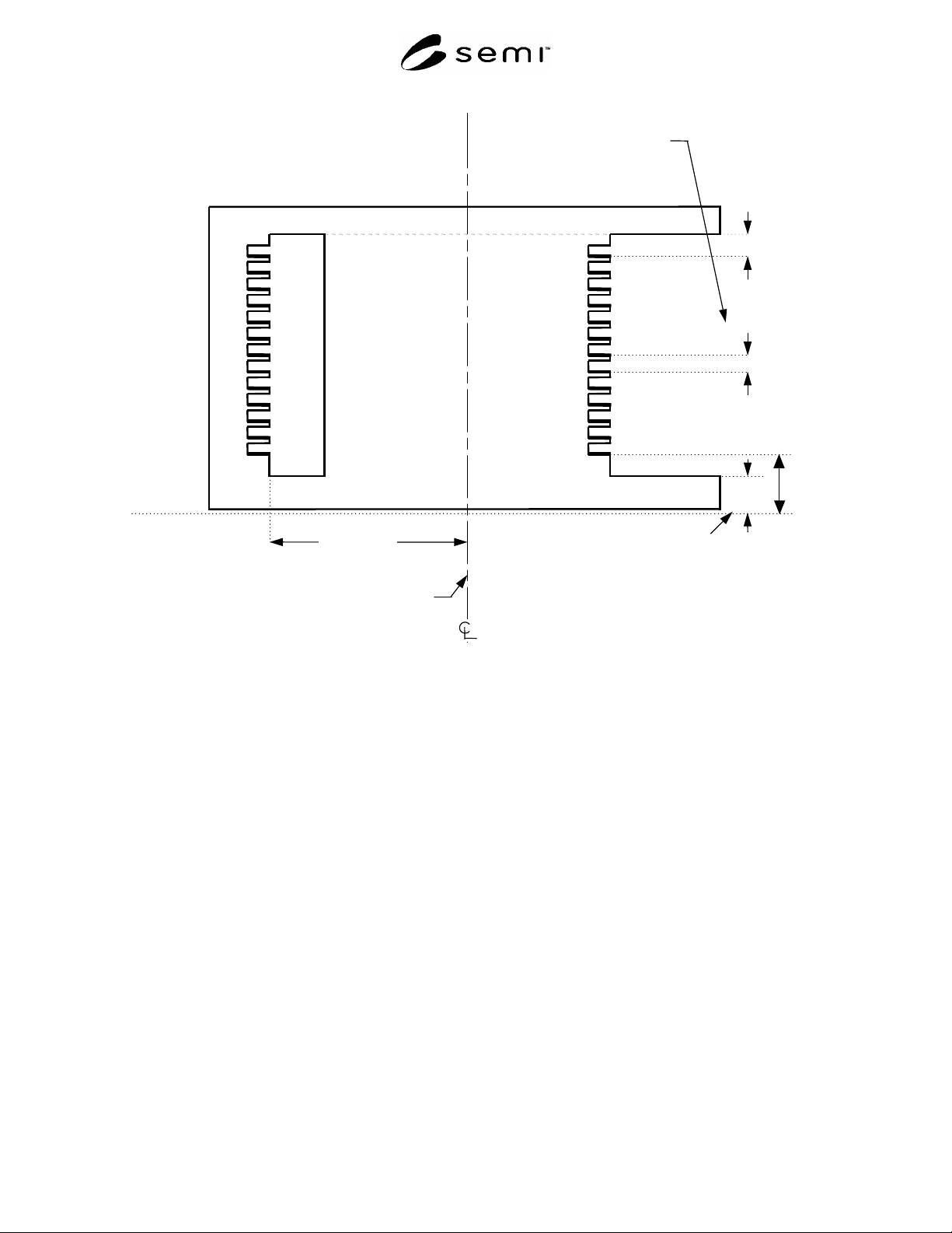
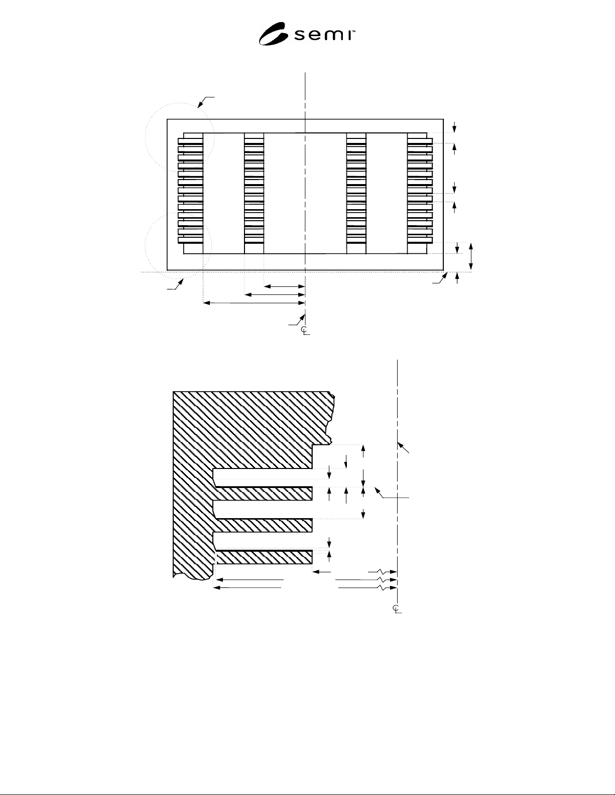
5.7 Internal Vertical Dimensions — Figures 2 through
5 show the vertical dimensions of the internal FOBIT.
Note that z8 (the height of the bottom nominal wafer-
seating plane above the horizontal datum plane) and z12
(the distance between adjacent nominal wafer seating
planes) are given as absolute distances with no
tolerance. This means that the sum of actual height
variations in the FOBIT from the kinematic coupling to
the supporting features holding each wafer must be
contained within the tolerance of z10 with no further
stack-up at each higher wafer. The method for meeting
this requirement is left up to the FOBIT supplier. Table
1 defines all dimensions for Figures 2 through 5.
y
1
3
facial
datum
p
lane
x
1
50
x
2
7
5
bilateral
datum
p
lane
r
4
170
ri
g
ht rear
side domain
left rea
r
side domain
front side of the FOBIT where wafers are accessed
left front
side domain
wafer
p
ick-u
p
area
ri
g
ht front
side domain
wafer set-
down and
extraction
volumes
r
2 = 152
r
3
r
2 + 1
+1
–
0
y
51
140
x
52
170
x
51
140
x
3
125
y
52
166
y
49
134
y
11
85
y
5
120
r
1
151
Figure 1
Top View of FOBIT Internal Dimensions
SEMI E119-1104 © SEMI 2002, 2004 5
horizontal datum plane
z8
=35
z6
28.5
z12
= 6.25
z15
4.6
facial datum plane
front side of the FOBIT where wafers
are accessed
y5 120
Figure 2
Side View of FOBIT Internal Dimensions
SEMI E119-1104 © SEMI 2002, 2004 6
z
4.6
x
1
50
x
2
75
x
3
125
Detail in
Figure 5
Detail in
Figure 4
horizontal datum plane
z 8
= 35
15
z 6
28.5
z
12
= 6.25
bilateral datum plane
Figure 3
Front View of FOBIT Internal Dimensions
z
23
1.5
z
11
2.9
z
12 = 6.25
x
3
125
bilateral
datum
plane
top
nominal
wafer
plane
z
z
10 = ± 0.5
(height of
wafer bottom)
r
2 = 152
r3
r2 + 1
+1
–0
z
15
4.6
Figure 4
Upper Cross-Section at Facial Datum Plane
5.7.1 Wafer Set-Down Volume — The open space for
the wafer set-down volume consists of a cylindrical
section with radius r2 and a main axis parallel to and y1
in front of the nominal wafer centerline. The top of this
cylindrical section is z11 above the nominal wafer-
seating plane and its bottom is z10 above the nominal
wafer-seating plane. The implications for wafer
positioning of the tolerance on r2 are as follows. The
wafers should be placed in the FOBIT within a circle of
radius corresponding to the smaller bound on r2 to
avoid touching the edge of the wafer to the side of the
FOBIT. Once the wafer has been placed, the FOBIT