semi合集-English.pdf - 第7519页
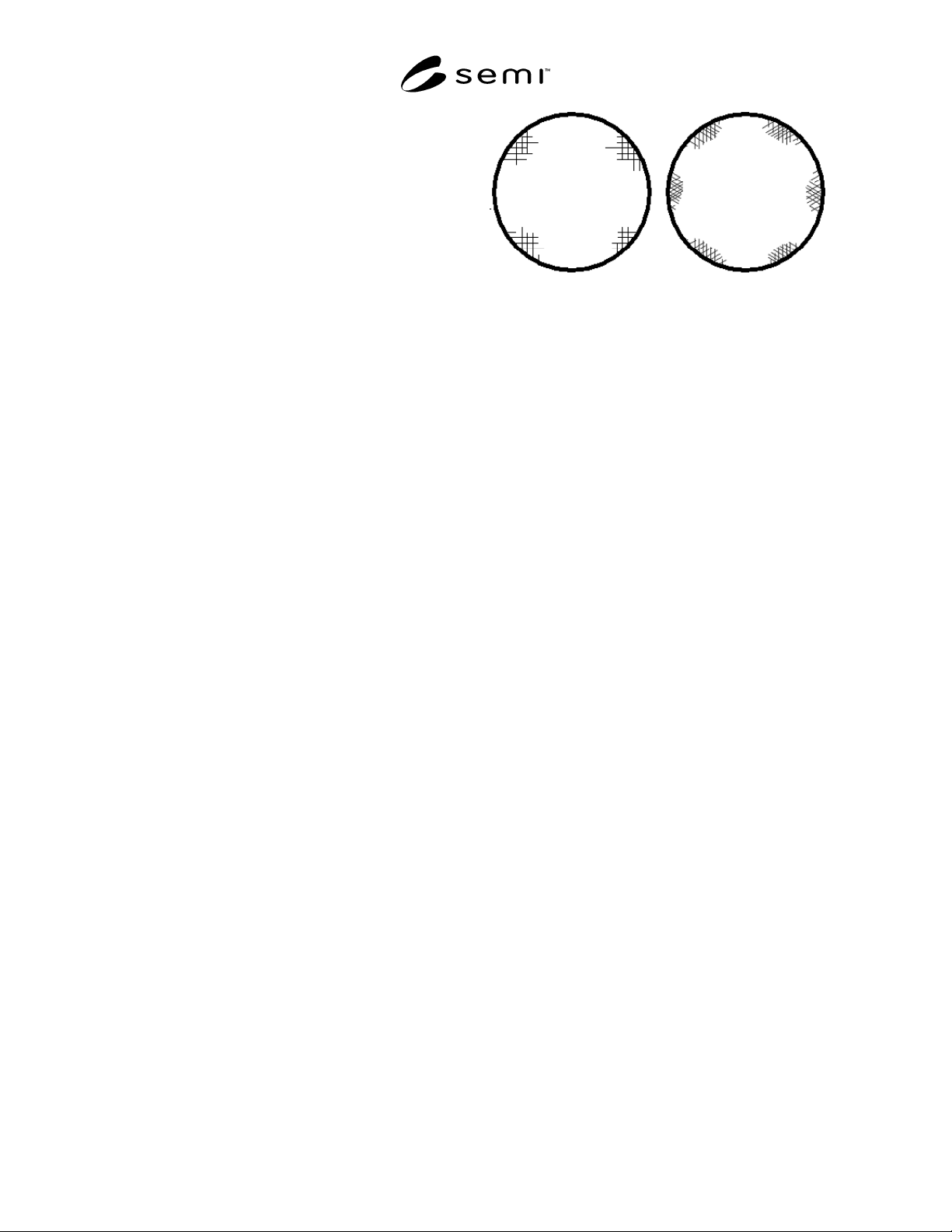
SEMI MF1726-1103 © SEMI 2003 3 a b NOTE: The orientation of the wafer does not define the locations and direction of the line defects. Figure 2 Typical Scratches (a) or Mechanically Induced Defects (b) as Seen With High-…
SEMI MF1726-1103 © SEMI 2003 2
wafers may also be microscopically inspected before
etching to count and classify visible imperfections.
Wafers are then etched in a preferential defect etchant
solution. The etched surface is again examined under
bright light illumination to identify patterns that may be
related to contamination or improper handling. The
imperfections highlighted by the preferential etchant are
then microscopically counted and classified.
6 Apparatus
6.1 Safety Equipment and Facility — for defect etching
as described in SEMI MF1809.
6.2 Wafer Inspection Facilities and Handling
Equipment — consistent with industry practice and
suitable for use with SEMI MF523.
7 Reagents and Materials
7.1 Refer to SEMI MF1809 for specific information on
reagents and materials.
8 Procedure
8.1 Select an unprocessed, polished or epitaxial wafer,
ready for use in the fabrication of electronic devices.
8.1.1 Open the wafer container in a particle-controlled
environment.
8.1.2 Transfer the wafer with a robotic tool or a
nonmetallic vacuum pencil, contacting the wafer edge
or back surface. Ensure that the front surface of the
adjacent wafer is not contacted during the removal.
NOTE 1: Any contact with the front surface of the adjacent
wafer can transfer contamination and generally scratch the
surface.
8.2 Preliminary Sample Inspection:
8.2.1 Inspect the first sample using high intensity light
conditions as described in SEMI MF523 to identify any
surface imperfections, scratches, or contamination
hazes that may interfere with the etching process or
confound the result. If any of these interferences are
detected, select a separate sample for analysis.
NOTE 2: These interferences can generate artifacts that may
be confused with the true defects.
8.2.2 Epitaxial Wafer, Nondestructive Defect Counting
— Inspect epitaxial wafers microscopically in
accordance with SEMI MF1810 before defect etching
to count most of the epitaxial stacking fault defects.
{100} {111}
NOTE: The orientation of the wafer defines the location and
direction of the line defects.
Figure 1
Slip Defects as Seen with Macroscopic High-
Intensity Light Inspection
NOTE 3: Epitaxial defects are more clearly delineated with
etching, but that is a destructive process.
8.3 Defect Etching
8.3.1 Epitaxial Wafers — Etch samples with epitaxial
layers greater than 2-µm thickness (as measured by
SEMI MF95) with removal of at least 0.5 µm to
highlight the crystal defects for quantification. Etch
samples with epitaxial layers less than 2 µm with
removal of no more than 50% of the layer thickness.
Other removal amounts are acceptable based upon
producer-consumer agreement. (See Note 4.)
8.3.2 Polished Wafers — The sample must be etched
with a removal of 5 to 15 µm to highlight the crystal
defects for quantification. Other removal amounts are
acceptable based upon producer/consumer agreement.
8.3.3 Refer to SEMI MF1809 for more etching
information.
NOTE 4: Crystal defects become more clearly visible for
unaided eye inspection with increased removal, but resolution
of the epitaxial induced defects is reduced with increasing
etch times.
8.4 Sample Inspection — Evaluate the preferentially
etched sample in two stages, macroscopic and
microscopic.
8.4.1 First inspect the sample macroscopically under
high intensity light conditions as described in
SEMI MF523 to detect patterns of defects, such as the
slip patterns shown schematically in Figure 1.

SEMI MF1726-1103 © SEMI 2003 3
a b
NOTE: The orientation of the wafer does not define the
locations and direction of the line defects.
Figure 2
Typical Scratches (a) or Mechanically Induced
Defects (b) as Seen With High-Intensity Light
Inspection
8.4.2 Obtain a second sample if evidence of
mechanically or operator induced damage or
contamination is observed, because these artifacts
interfere with the identification of crystal growth
defects.
NOTE 5: Slip defects may be differentiated from the crystal
growth defects by insuring that all of the defects are aligned
as shown in Figure 1. Figure 2 shows the characteristics of
scratches or mechanical damage when viewed under high
intensity light conditions.
8.4.3 Microscopic Defect Counting — Count and report
the density of observed defects using SEMI MF1810.
9 Keywords
9.1 dislocation; epitaxy; grain boundaries; hillock;
polycrystalline imperfections; preferential etch; shallow
pit; silicon; slip; stacking fault
NOTICE: SEMI makes no warranties or
representations as to the suitability of the standards set
forth herein for any particular application. The
determination of the suitability of the standard is solely
the responsibility of the user. Users are cautioned to
refer to manufacturer' s instructions, product labels,
product data sheets, and other relevant literature,
respecting any materials or equipment mentioned
herein. These standards are subject to change without
notice.
By publication of this standard, Semiconductor
Equipment and Materials International (SEMI) takes no
position respecting the validity of any patent rights or
copyrights asserted in connection with any items
mentioned in this standard. Users of this standard are
expressly advised that determination of any such patent
rights or copyrights and the risk of infringement of such
rights are entirely their own responsibility.
Copyright by SEMI® (Semiconductor Equipment and Materials
International), 3081 Zanker Road, San Jose, CA 95134. Reproduction o
f
the contents in whole or in part is forbidden without express written
consent of SEMI.

SEMI MF1727-0304 © SEMI 2003, 2004 1
SEMI MF1727-0304
PRACTICE FOR DETECTION OF OXIDATION INDUCED DEFECTS IN
POLISHED SILICON WAFERS
This practice was technically approved by the Global Silicon Wafer Committee and is the direct
responsibility of the North American Silicon Wafer Committee. Current edition approved for publication by
the North American Regional Standards Committee on December 4, 2003. Initially available at
www.semi.org February 2004; to be published March 2004. Originally published by ASTM International as
ASTM F 1727-97. Last previous edition SEMI MF1727-02.
1 Purpose
1.1 Defects induced by thermal processing of silicon
wafers may adversely influence device performance
and yield.
1.2 These defects are influenced directly by
contamination, ambient atmosphere, temperature, time
at temperature, and rate of change of temperature to
which the specimens are subjected. Conditions vary
significantly among device manufacturing technologies.
The thermal cycling procedures of this practice are
intended to simulate basic device processing
technologies. Oxidation cycles other than specified
herein, or multiple oxidation cycles, may sometimes
more accurately simulate device-processing procedures.
The results obtained may differ significantly from those
obtained with the specified oxidation cycles.
1.3 The geometry of some patterns revealed by this
practice suggests that they are related to the crystal
growth process while others seem related to surface
preparation or thermal cycling conditions.
1.4 This practice is suitable for acceptance testing
when used with referenced practices and methods.
2 Scope
2.1 This practice covers the detection of crystalline
defects in the surface region of silicon wafers. The
defects are induced or enhanced by oxidation cycles
encountered in normal device processing. An
atmospheric pressure oxidation cycle representative of
bipolar, metal-oxide-silicon (MOS) and CMOS
technologies is included. This practice reveals strain
fields arising from the presence of precipitates,
oxidation induced stacking faults, and shallow etch pits.
Slip is also revealed that arises when internal or edge
stresses are applied to the wafer.
2.2 Application of this practice is limited to specimens
that have been chemical or chemical/mechanical
polished to remove surface damage from at least one
side of the specimen. This practice may also be applied
to detection of defects in epitaxial layers.
2.3 The surface of the specimen opposite the surface to
be investigated may be damaged deliberately or
otherwise treated for gettering purposes or chemically
etched to remove damage.
NOTICE: This standard does not purport to address
safety issues, if any, associated with its use. It is the
responsibility of the user of this standard to establish
appropriate safety and health practices and determine
the applicability of regulatory or other limitations prior
to use.
3 Limitations
3.1 Material having residual work damage in the
polished surface exhibits visible patterns when the
procedures of this practice are used. Usually, edge
damage, lapping damage, tool marks, or scratches are
easily identified by the location and pattern observed.
3.2 Contamination not removed by preparatory
cleaning procedures or deposited following cleaning,
may become visible after oxidation and preferential
etching.
3.3 Slip may be introduced by differential expansion at
the points of wafer support in the furnace boat. Slip
radiating from the points of support may be assumed to
originate from this boat pinch and not be inherent in the
unprocessed wafer. Slip may also be caused by large
thermal gradients imposed across a wafer by fast
insertion or removal from the furnace.
3.4 If the oxidation furnace or apparatus is
contaminated, it can cause extraneous artifacts or
defects.
3.5 Striations, helical features on the surface of a
silicon wafer, are ascribed to periodic dopant
incorporation differences occurring at the rotating solid-
liquid interface during crystal growth. These features
are visible to the unaided eye after preferential etching,
seem continuous under 100× magnification, and may be
confused with ring patterns of oxidation stacking faults.
3.6 Otherwise identical wafers with different back
surface conditions may yield different results by this
practice.