semi合集-English.pdf - 第31页
SEMI E1.9-0701 E2 © SEMI 1994, 2004 11 lower tolerance of z 10 around the nominal wafer seating plane. 6.7.4 To prevent wafers from creeping out of the cassette during transport, the fork-lift area may be slanted so that…
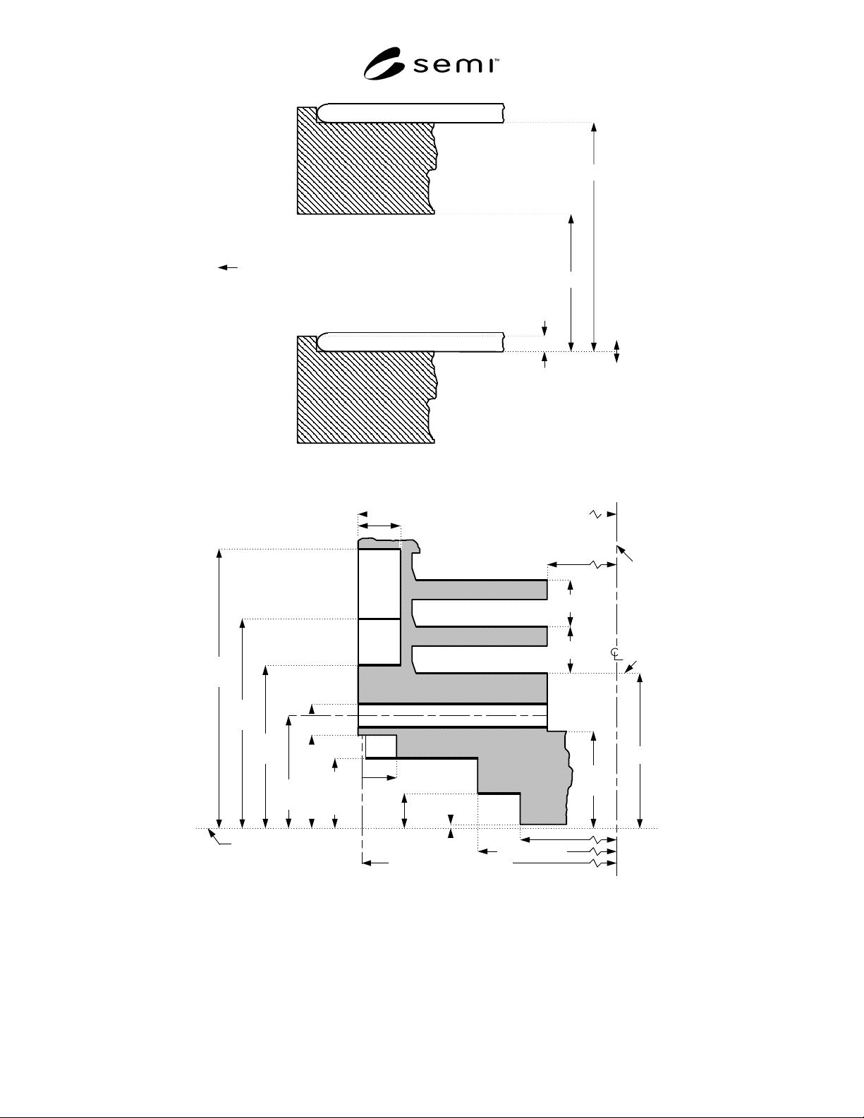
SEMI E1.9-0701
E2
© SEMI 1994, 2004 10
Wafer
z10
=±0.5
z29
≤
0.7
z12 =10
z11
≥
6
front side of the cassette where wafers are accessed
Figure 11
Optional Feature to Prevent Wafer Creep-Out
z3
=7±1
z9
=45±1
z8 =33
x3 ≥125
z12 =10
z12 =10
bilateral
datum
plane
z19
=24
z7
=35±1
horizontal datum plane
z6
≤21
z4
=15±1
(if ω=0)
z1 ≥0
z2 ≤2
(at sensor pad)
x9 ≤167
x10 =166±1 (at side grip pits)
x15 ≤132
x16 =140±1
z20
=60±1
r9 =2.5±0.5
r8 =7.5±1
x4 ≥8
bottom
nominal
wafer
plane
x11 =166 (to origin of r8)
z22
≥20
Figure 12
Lower Cross-Section at Facial Datum Plane
6.7.3 If a wafer is placed in the wafer set-down volume
and is then pushed toward the rear of the cassette, then
the entire bottom of the wafer must be contained in the
wafer pick-up volume. However, if the wafer is not
pushed toward the rear of the cassette (or the cassette is
not tilted back during transport), then the wafer may
only be somewhere within the wafer extraction volume.
The wafer pick-up volume is defined by a cylindrical
section with radius r1 and a main axis at the nominal
wafer center line. Its top and bottom are the upper and
SEMI E1.9-0701
E2
© SEMI 1994, 2004 11
lower tolerance of z10 around the nominal wafer
seating plane.
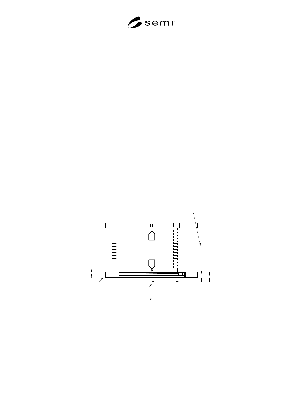
6.7.4 To prevent wafers from creeping out of the
cassette during transport, the fork-lift area may be
slanted so that the front of the cassette is higher than the
rear. Specifically, the surface defined by z4 may be
rotated by an angle ω about the line where z4 intersects
y29 (as shown in Figure 13). Only the surface behind
y29 may be rotated. Thus, the height of z4 shown in
Figure 12 might only be defined at y29, and z4 can be
greater than 15 ± 1 behind y29. However, the flatness of
the resulting tilted surface must still fall within the
tolerance given for z4.
6.8 Cassette Identification Tag Area — The following
areas are provided for putting identification tags on the
cassette. Examples of such tags include thin electronic
modules and printed labels designed to be read by
either humans or machines. It is recommended that
such tags be contained within the 18 mm by 60 mm
(0.71 in. by 2.36 in.) region defined when the bounds
are tight. It is also recommended that if such tags are
smaller than the minimum bounds of the tag area, they
should be centered within those bounds.
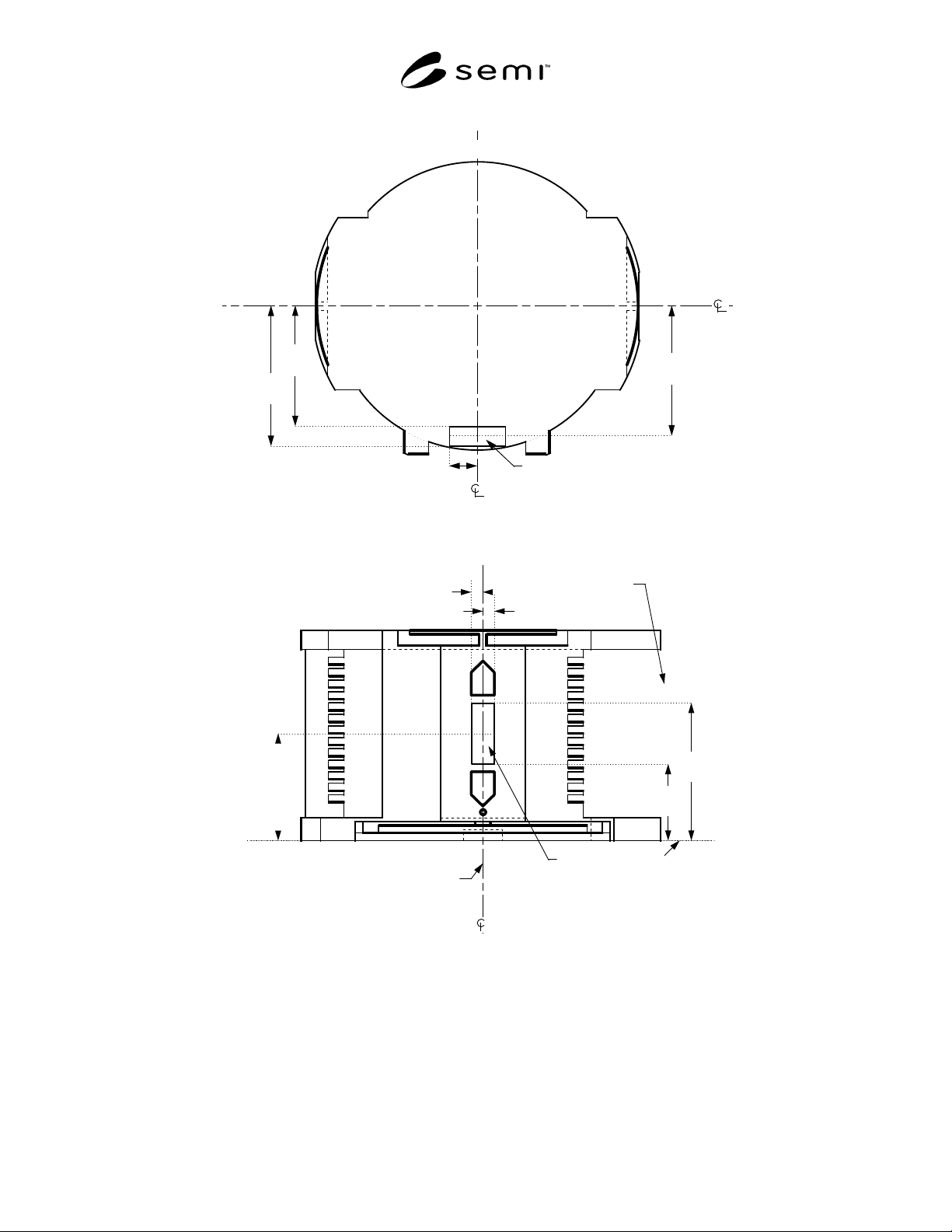
6.8.1 An optional place for an identification tag on the
top of the cassette is shown in Figure 14. Although the
height of this surface is not specified, the surface must
be completely visible from above. The parallelism of
the top identification tag with respect to the horizontal
datum plane is given by z25. It is recommended that the
identification tag should be centered on the bilateral
datum plane at a point y21 behind the facial datum
plane.
6.8.2 An optional place for an identification tag on the
right-hand side of the cassette is shown in Figure 15
(where “right-hand” is defined as the right side of the
cassette when it is oriented correctly and it is viewed
from the rear). Although the left-right location of this
surface is not specified, the surface must be completely
visible from the right of the cassette. The parallelism of
the side identification tag with respect to the bilateral
datum plane is given by x27. It is recommended that the
identification tag should be centered on the facial datum
plane at a point z99 above the horizontal datum plane.
6.8.3 An optional place for an identification tag on the
bottom of the cassette is shown in Figure 16. Although
the height of this surface is not specified, the surface
must be completely visible from below. The parallelism
of the bottom identification tag with respect to the
horizontal datum plane is given by z25. It is
recommended that the identification tag should be
centered on the bilateral datum plane at a point y22
behind the facial datum plane.
z4
=15±1
horizontal
datum
plane
y29 =89
(to axis of rotation)
facial datum plane
0° ≤ ω ≤ 2°
front side of the cassette where
wafers are accessed
z3
=7±1
Figure 13
Slanting of Fork-Lift Area
SEMI E1.9-0701
E2
© SEMI 1994, 2004 12
y26
≥145
facial
datum
plane
front side of the cassette where wafers are accessed
y25
≤127
bilateral datum plane
x25 ≥30
cassette
identification
tag area
y21
=136
Figure 14
Optional Top Cassette Identification Tag Area
z28
≥124.5
horizontal
datum
plane
z27
≤64.5
facial datum plane
y27
≥9
y28
≥9
cassette
identification
tag area
front side of the cassette where
wafers are accessed
z99
=94.5
Figure 15
Optional Side Cassette Identification Tag Area