semi合集-English.pdf - 第6122页
SEMI G26-90 © SEMI 198 3, 1996 2 5 Dimension s and Perm issi b l e Var iations The lid dimensions shall confor m as specified in Figure 3 and Table 1. Figure 3 Dimensions Table 1 Lid Dimen sions for 0.050" Pad Cente…
SEMI G26-90 © SEMI 1983, 19961
SEMI G26-90
SPECIFICATION FOR HERMETIC SLAM CHIP CARRIER LIDS
1 Preface
This specification covers the ceramic piece part
commonly referred to as a lid, used in the construction
of a hermetic SLAM package with a .050" pad
centerline. The SLAM package is covered separately in
the SEMI G5 Specification for Ceramic Chip Carriers.
2 Applicable Documents
MIL-STD-883
1
— Test Methods and Procedures for
Microelectronics
MIL-M-38510 — General Specification for
Microcircuits
MIL-I-23011 — Iron Nickel Alloys for Sealing to Glass
and Ceramic
3 Selected Definitions
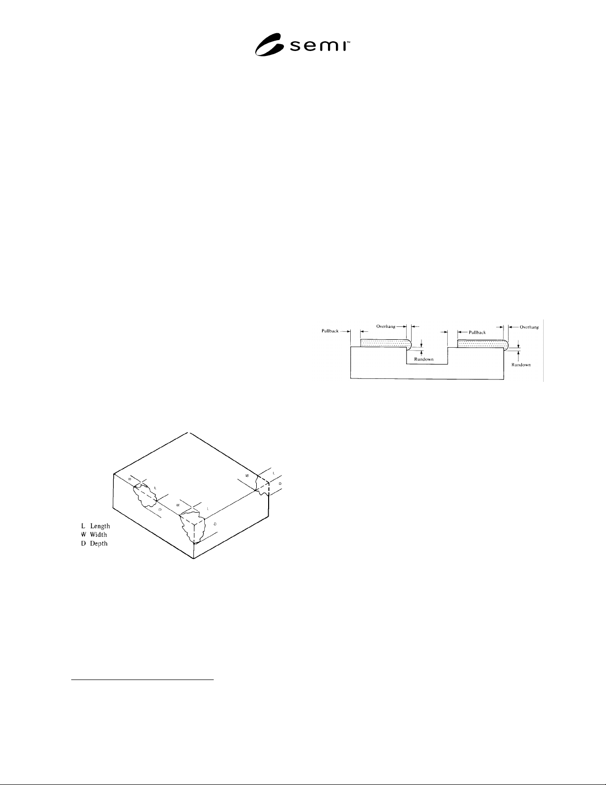
burr — A fragment of excess material or foreign
particle adhering to the surface.
chip — Region of ceramic missing from the surface or
edge of a package which does not go completely
through the package. Chip size is given by its length,
width and depth from a projection of the design plan-
form (see Figure 1).
Figure 1
Chip Illustration
crack — A cleavage or fracture that extends to the
surface of a package. It may or may not pass through
the entire thickness of the package.
1 Military Standards, Naval Publications and Form Center, 5801
Tabor Ave., Philadelphia, PA 19120
fin — A fine, feathery-edged projection on the edge or
corner of the ceramic.
glass flow — Heated just sufficiently to remove all
screen mesh marks visible at 10× magnification.
overhang — Horizontal extension of glass from the
ceramic.
projection — Raised portion of the surface indigenous
with the parent material.
pullback — Defines a dimension covering the linear
distance between the edge of the ceramic and the first
measurable glass interface excluding any glass spatter
(see Figure 2).
rundown — Vertical extension of glass from the
ceramic (see Figure 2).
Figure 2
Glass Misalignment
seal area — A dimensional outline area designated for
sealing the lid and package together.
terminal — Case outline at point of entry or exit of an
electrical contact.
void —An absence of glass from a designated glassed
area on the ceramic surface.
4 Ordering Information
Purchase orders for SLAM lids furnished to this
specification shall include the following items:
1. Drawing number and revision level
2. Type and color of ceramic
3. Type and thickness of sealing material
4. Length, width, thickness and sealing area
5. Certification
6. Method of test and measurements (see Section 9)
7. Lot acceptance procedures (see Section 8)
8. Packaging and marking (see Section 10)
SEMI G26-90 © SEMI 1983, 1996 2
5 Dimensions and Permissi ble Variations
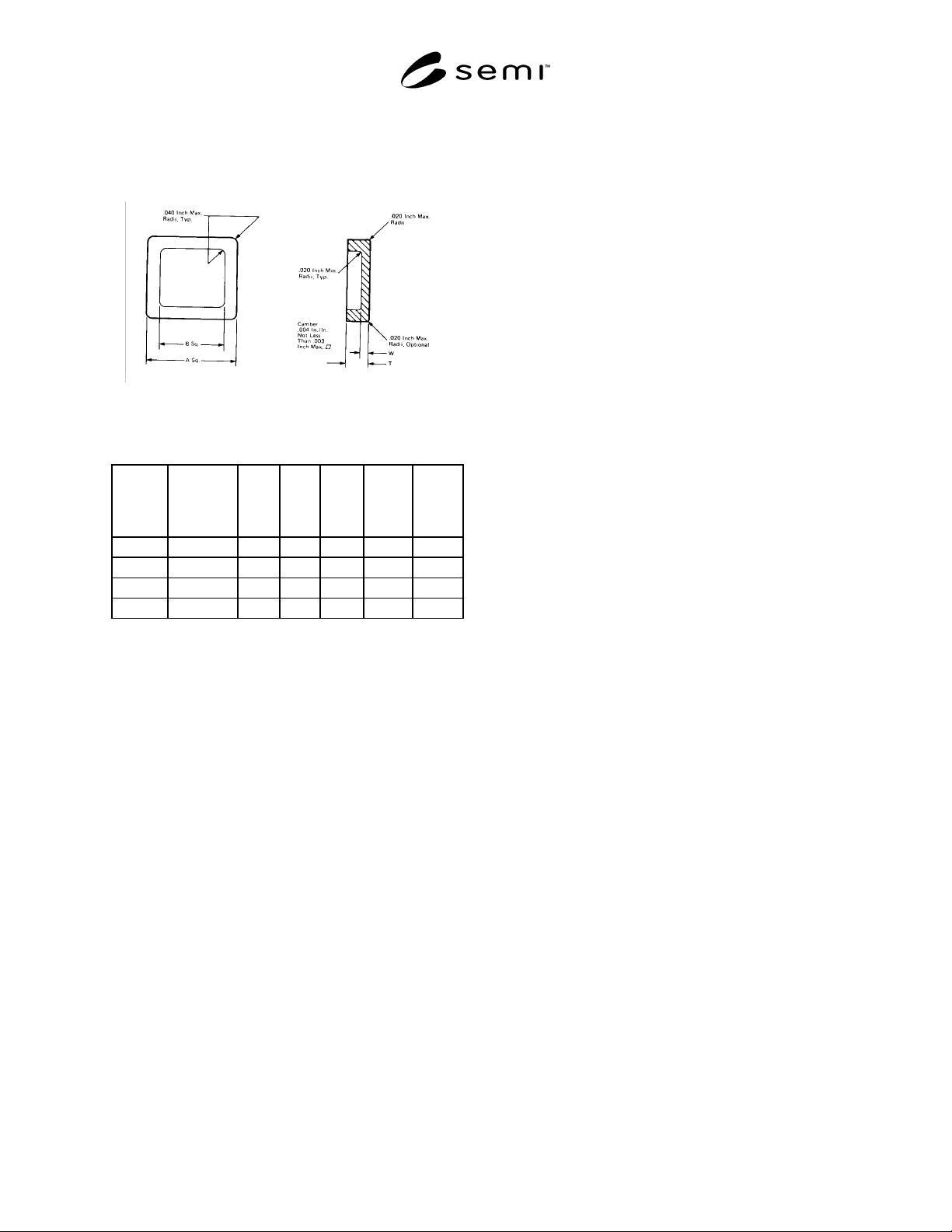
The lid dimensions shall conform as specified in Figure
3 and Table 1.
Figure 3
Dimensions
Table 1 Lid Dimensions for 0.050" Pad Centerline
Terminals
Chip Carrier
Base
Thickness
(Reference) DIM A DIM B DIM T DIM W
S/R,
WIDTH
20 0.020 0.310 0.230 0.060 0.020 0.040
28 0.025 0.410 0.330 0.060 0.025 0.040
44 0.040 0.500 0.420 0.065 0.025 0.040
68 0.040 0.700 0.560 0.065 0.022 0.070
6 Materials
6.1 Ceramic
6.1.1 Alumina content 90% minimum or Beryllia
content 94% minimum.
6.1.2 Dark or white.
6.2 Sealing Material — As specified in the ordering
information.
7 Defect Limits
7.1 Ceramic
7.1.1 Cracks — Cracks are not allowed.
7.1.2 Chips
7.1.2.1 Corner — 0.762 mm × 0.762 mm × 0.762 mm
(0.030" × 0.030" × 0.030").
7.1.2.2 Edge — 0.762 mm × 0.762 mm × 0.762 mm
(0.030" × 0.030" × 0.030").
7.1.2.3 Chips cannot reduce the seal path by more than
0.381 mm (0.015") or 10%, whichever is smaller.
7.1.3 Burrs, Projections, and Fins — Lids — 0.127
mm (0.005") maximum.
7.1.4 Camber — 0.004 inch/inch. For sizes below one
inch the maximum camber shall be 0.076 mm (0.003").
7.2 Glass
7.2.1 Chips or Voids — There shall be no chips or
voids after glass flow test.
7.2.2 Glass Misalignment — (As received.)
7.2.2.1 External Overhang — 0.254 mm (0.010")
maximum.
7.2.2.2 External Rundown — 30% of ceramic
thickness maximum at maximum material condition.
7.2.2.3 Glass Pullback — 0.254 mm (0.010")
maximum.
7.2.2.4 Regardless of maximum allowable criteria
stated above, the seal area must not be reduced by
greater than 20% of the nominal design width.
7.2.3 Glass thickness shall be measured in four
locations. Measurement shall be made on glass and
base total thickness. Base reference thickness shall be
measured on the same part by removal of a portion of
the glass.
7.2.4 Glass splatter in all areas may not exceed 0.052
mm (0.002") in height, 0.127 mm (0.005") in diameter,
with a maximum of three per 0.1" square area on the
cavity surface.
8 Sampling
Sampling will be determined between supplier and
purchaser.
9 Test Methods
9.1 Sequence of Events and Functional Testing —
During functional testing, the sequence of testing shall
be:
1. Seal
2. Vapor Content
3. Environmental Testing
4. Fine Leak
5. Gross Leak
6. Torque Test
9.2 Hermetic and Environmental Testing
9.2.1 The hermetic integrity of the package must be
maintained after all environmental testing. Hermetic
checks shall comply with MIL-STD-883, Method 1014,
Test Conditions A
1
, or B and C.
9.2.2 Environmental testing shall include: Temp
Cycle, MIL-STD-883, Method 1010, Condition C.

SEMI G26-90 © SEMI 1983, 19963
10 Packaging and Marking
10.1 Packaging — Containers selected shall be strong
enough and suitably designed to provide maximum
protection against crushing, spillage and other forms of
damage to the container or its contents. Containers shall
afford protection of the contents to contamination from
exposure to excessive moisture or oxidation by gases.
Packaging materials shall be so selected to prevent any
contamination of the ceramic component parts with
paper fibers or organic particles.
10.2 Marking — The outer containers shall be clearly
marked to identify the user stock number, user purchase
order number, drawing number, quantity, vendor lot
number, and solder glass type.
NOTICE: These standards do not purport to address
safety issues, if any, associated with their use. It is the
responsibility of the user of these standards to establish
appropriate safety and health practices and determine
the applicability of regulatory limitations prior to use.
SEMI makes no warranties or representations as to the
suitability of the standards set forth herein for any
particular application. The determination of the
suitability of the standard is solely the responsibility of
the user. Users are cautioned to refer to manufacturer’s
instructions, product labels, product data sheets, and
other relevant literature respecting any materials
mentioned herein. These standards are subject to
change without notice.
The user’s attention is called to the possibility that
compliance with this standard may require use of
copyrighted material or of an invention covered by
patent rights. By publication of this standard, SEMI
takes no position respecting the validity of any patent
rights or copyrights asserted in connection with any
item mentioned in this standard. Users of this standard
are expressly advised that determination of any such
patent rights or copyrights, and the risk of infringement
of such rights, are entirely their own responsibility.
Copyright by SEMI® (Semiconductor Equipment and Materials
International), 3081 Zanker Road, San Jose, CA 95134. Reproduction o
f
the contents in whole or in part is forbidden without express written
consent of SEMI.