semi合集-English.pdf - 第6522页
SEMI G80-0200 © SE MI 2000 30 A P PENDIX 3 EXCEPTIONS PA GE NOTE: T he material in this appe ndix is an of ficial part of SEMI G80 and wa s approved by f ulll letter ballot proced ures on Septem ber 3, 1999 by the North …
SEMI G80-0200 © SEMI 200029
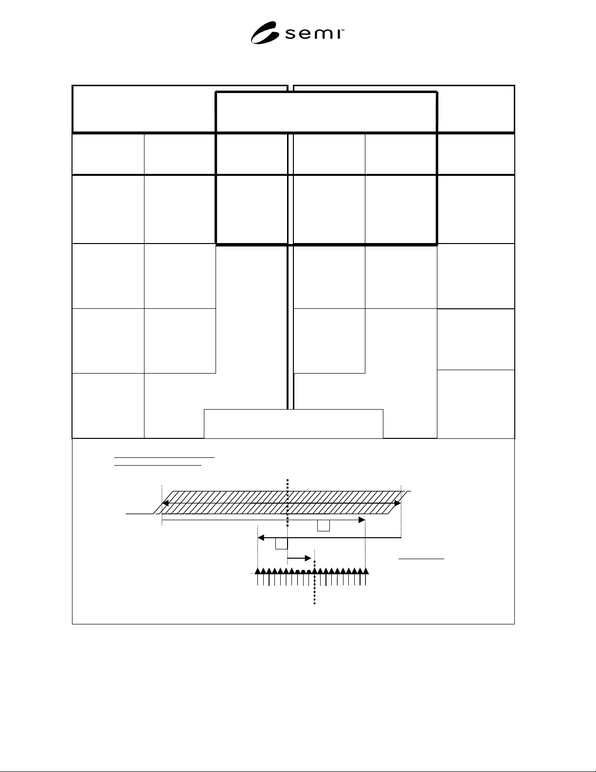
Example A2-6 Test Method Summary for Showing Data Entry to Table 2 for OTA Calculation
LEVEL 1
Timin
g
Linearit
y
Ext. Dly. / Mult Period
Data below represents
Level 1 edge-delay
results
LEVEL 2
Hi
g
h S
p
eed Clock
Accuracy
_
_________________
_
Drive Input Z Timing
Error Level 1
(Section 10.3.5) Z to
0 (Low)
Timing Linearity
Level 1 (Sec.10.3.1)
Positive Error:
+350
Negative Error:
–250
b) High Speed Clock
Transition Time
Variation Level 2
(Section 10.4.3- Drive
Input Transition Time
for clock function)
a) High Speed Clock
Delay Error
Level 2 (Section 10.4.1-
Drive Input Timing
Delay for clock
function)
Extended Delay
Level 1 (Sec. 10.3.4)
Positive Error:
Negative Error:
Multiple Period
Level 1 Optional
(Sec. 10.3.6)
Positive Error:
Negative Error:
Drive Input Z Timing
Error Level 1
(Section 10.3.5) Z to
1 (High)
Drive Input Z Timing
Error Level 1
(Section 10.3.5) 0
(Low) to Z
Drive Input Z Timing
Error Level 1
(Section 10.3.5) 1
(High) to Z
1) Drive In
p
ut To
Compare Output
Timing
+50
3) Com
p
are Out
p
ut
Edge Placement
±100
2) Drive
Input Edge
Placement
± 200
Drive Input to
Compare Out put
Timing Accuracy
Taken from Section
10.3.1
+50
a) Compare Output
Time Delay Error
Level 2 (Section
10.4.2)
± 100
a) Drive Input Timing
Delay Error Level 2
(Section 10.4.1)
± 200
b) Drive Input
Transition Time
Variation
Level 2 (Section
10.4.3)
c) Drive Input Timing
Cycle Jitter Level 2
(Section 10.4.4)
Single Point Overall Timing Accuracy (OTA) Results
D
ata to enter here is: A = Dr (item 2) + Cmp (item 3) + Dr-Cmp (item 1)
-B = -Dr (item 2) - Cmp (item 3) + Dr-Cmp (item 1)
.
+350ps, –250ps
Drive Z Timin
g
Data below
represents Level 1 Z-
state timing results
c) High Speed Clock
Cycle Jitter Level 2
(Section 10.4.5)
d) High Speed Clock
Phase Jitter Level 2
(Section 10.4.6)
The user of the method is advised to read Section 13,
Precautions before filling in this table.
-200ps
Drive Edges
1000ps
+200ps
OTA Calculation:
OTA = A, -B
A = Dr + Cmp + Dr-Cmp
200 + 100 + 50 = 350
-B = -Dr - Cmp + Dr-Cmp
-200 - 100 + 50 = -250
OTA = 350, –250
1050ps
OTA DATA CALCULATION and
TABLE 2 ENTRY EXAMPLE
800ps 1200ps
Drive edges programmed
value of 1000ps
+100ps-100ps
Compare Edges
B- Latest drive to earliest compare: -250ps
50ps
B
A- Earliest drive to latest compare: 350ps
Compare edges programmed
value of 1000ps
A
950ps 1150ps
350ps
-250ps
SEMI G80-0200 © SEMI 2000 30
APPENDIX 3
EXCEPTIONS PAGE
NOTE: The material in this appendix is an official part of SEMI G80 and was approved by fulll letter ballot procedures on
September 3, 1999 by the North Amerian Regional Standards Committee.
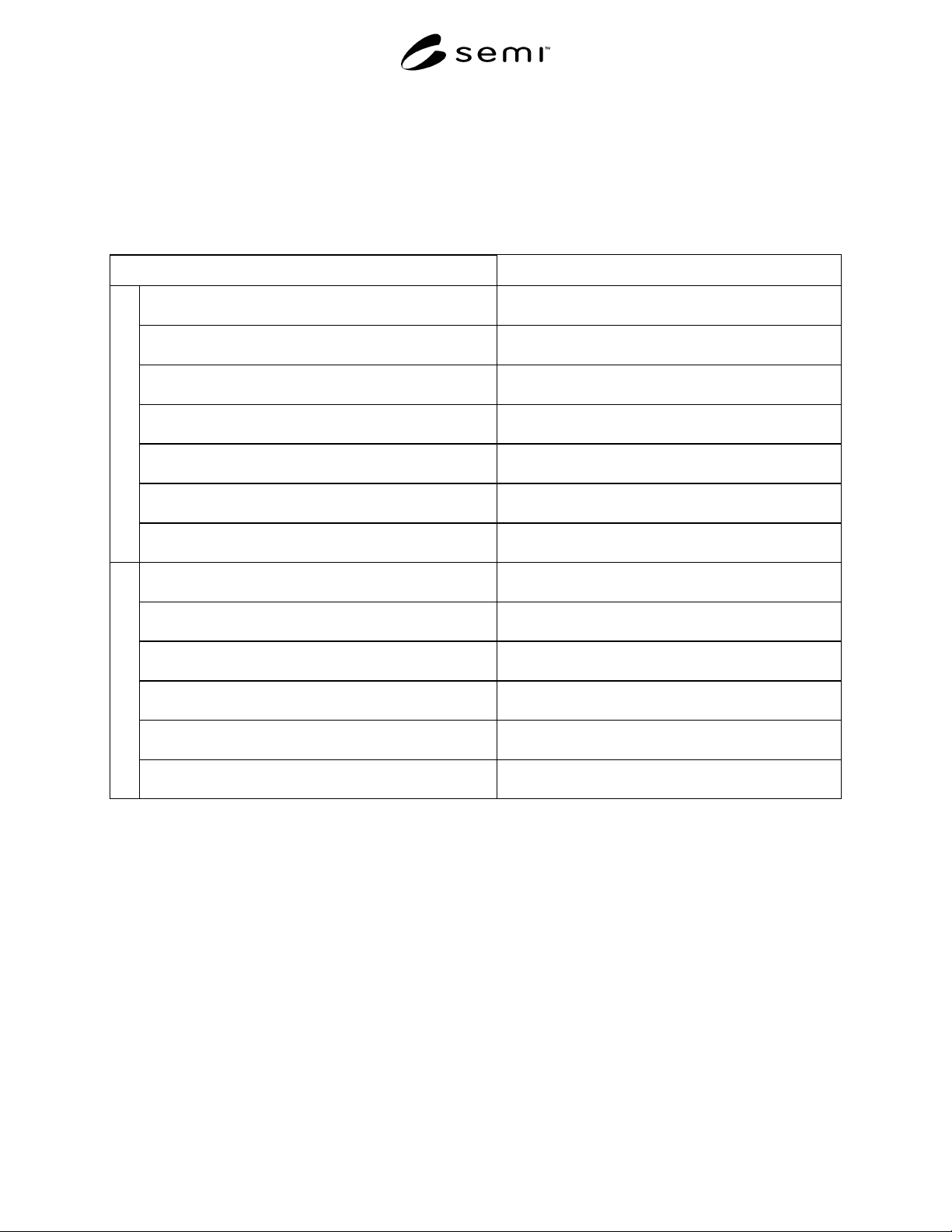
NOTE 2: This page is intended to capture any Digital Timing Accuracy Analysis Method exceptions the user has chosen to
make.
Test Number NOTE 3: MAKE ATTACHMENTS AS NEEDED
Section 10.3.1 Timing Linearity Test
(Drive Input Edge Placement)
Section 10.3.4 Extended Delay Test
(Compare Output Edge Placement)
Section 10.3.5 Drive Input Z Timing Error
(Z to 0 (Low))
Section 10.3.5 Drive Input Z Timing Error
(Z to 1 (High))
Section 10.3.5 Drive Input Z Timing Error
(0 (Low) to Z)
Section 10.3.5 Drive Input Z Timing Error
(1 (High) to Z)
L
E
V
E
L
O
N
E
Section 10.3.6 Multiple Period Test
(Optional- for on the fly timing)
Section 10.4.1 Drive Input Time Delay Error
(Drive Input Edge Placement)
Section 10.4.2 Compare Output Time Delay Error
(Compare Output Edge Placement)
Section 10.4.3 Drive Input Transition Time Variation
Section 10.4.4 Drive Input Timing Cycle Jitter
(Short term cycle to cycle period jitter)
Section 10.4.5 High Speed Clock Self Trigger Cycle Jitter
(Short term cycle to cycle period jitter/clocks)
L
E
V
E
L
T
W
O
Section 10.4.6 High Speed Clock Self Trigger Phase Jitter
(Short term phase/duty cycle jitter/clocks)
SEMI G80-0200 © SEMI 200031
APPENDIX 4
NOTE: The material in this appendix is an official part of SEMI G80 and was approved by fulll letter ballot procedures on
September 3, 1999 by the North Amerian Regional Standards Committee.
A4-1 Jitter Measurement
A4-1.1 If a jitter measurement described here is to be
statistically correct the jitter variation in the signal
being measured must be Gausian. The measured jitter
in this method will be represented as one standard
deviation (sigma) of the Gausian distribution, referred
to here as the RMS jitter value.
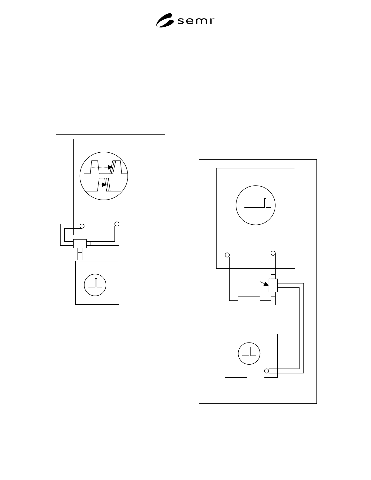
Signal Source
Sampling Oscilloscope
Trigger
Signal
Input
Coax
High frequency power splitter
Figure A4-1
Signal Jitter Measurement
A4-1.2 The signal being measured will have some
amount of jitter. The instrumentation used to measure
the jitter will also have some amount of jitter. To
accurately measure the jitter of a periodic signal the
jitter component of the instrumentation must be
accounted for and subtracted from the signal being
measured.
A4-1.3 Two jitter measurements are required. A jitter
measurement will be made on the signal of interest. A
second jitter measurement will be made to determine
the instrumentation jitter. Instrumentation jitter will be
subtracted from the signal measurement to obtain the
most accurate representation of signal jitter.
A4-1.4 A sampling oscilloscope will have an inherent
delay, typically on the order of 20ns. This represents
the time difference from the time the oscilloscope is
triggered to the time when an input signal can be
viewed. The key to extracting the jitter of the
measurement instrumentation is providing a setup that
allows viewing the trigger on the oscilloscope display.
This is accomplished by delaying the oscilloscope
trigger to an input channel.
Sampling Oscilloscope
Trigger
Input
Signal
Delay
(Semi-
rigid coax)
High frequency
power splitter
Coax
Pulse Generator
Output
Figure A4-2
Measuring Instrumentation Jitter