semi合集-English.pdf - 第7343页
SEMI MF1390-1104 © SEMI 2004 3 6.2 The wafer is supported by a sm a ll-area chuck with front surface up. 6.3 Both external surfaces a r e simultaneously scanned along a prescribed pat tern by an opposed pair of pr obes t…
SEMI MF1390-1104 © SEMI 2004 2
in diameter and thickness are shown in Related
Information 1. If the crystal orientation of the sample
to be measured differs from the crystal orientation of
the gravity-compensation wafer, then the measured
warp value may differ from the actual warp value by up
to 15%. Error tables for fiducial variation have not
been generated.
3.3 Different methods for implementing gravitational
compensation may give different results. Varying
levels of completeness of implementing a method may
also give different results.
3.4 Mechanical variations in wafer holding devices
between systems may introduce measurement
differences. This test method allows the use of a
variety of wafer holding devices (see Section 7.1.4.1);
results obtained with different geometrical
configurations of wafer holding device on the same test
samples may differ.
3.5 Most equipment systems capable of this
measurement have a definite range of wafer thickness
combined with warp (dynamic range) that can be
accommodated without readjustment. If the sample
moves outside this dynamic range during either
calibration or measurement, results may be in error. An
over-range signal can be used to alert the operator and
measurement data examiners to this event.
3.6 The quantity of data points and their spacing may
affect the measurement results. This test method does
not specify the data point spacing (see Section 7.1.4.2);
results obtained with different data point spacings on
the same test samples may differ.
4 Referenced Standards
4.1 SEMI Standards
SEMI M1 — Specifications for Polished
Monocrystalline Silicon Wafers
SEMI MF657 — Test Method for Measuring Warp and
Total Thickness Variation on Silicon Wafers by
Noncontact Scanning
SEMI MF1241 — Terminology of Silicon Technology
SEMI MF1530 — Test Method for Measuring Flatness,
Thickness, and Thickness Variation on Silicon Wafers
by Automated Non-contact Scanning
4.2 ASTM Standard
E 691 — Practice for Conducting an Interlaboratory
Study to Determine the Precision of a Test Method
2
2 Available from ASTM International, 100 Barr Harbor Drive, West
Conshohocken, PA 19428, Tel: 610-832-9500, Fax: 610-832-9555,
Website
http://www.astm.org. Appears in Volume 14.02 of Annual
Book of ASTM Standards.
NOTICE: Unless otherwise indicated, all documents
cited shall be the latest published versions.
5 Terminology
5.1 Definitions
5.1.1 mechanical signature, of an instrument — that
component of a measurement that is introduced by the
instrument and that is systematic, repeatable, and
quantifiable.
5.1.2 median surface, of a semiconductor wafer — the
locus of points equidistant from the front and back
surfaces of the wafer.
5.1.3 reference plane, of a semiconductor wafer — a
plane from which deviations of a specified surface of
the wafer are measured.
5.1.4 reference plane deviation (RPD) — the distance
from a point on a reference plane to the corresponding
point on a wafer surface.
5.1.4.1 Discussion — A dome-shaped wafer is
considered to have positive RPD at its center; a bowl-
shaped wafer is considered to have negative RPD at its
center.
5.1.5 thickness, of a semiconductor wafer — the
distance through the wafer between corresponding
points on the front and back surfaces.
5.1.6 warp, of a semiconductor wafer — the algebraic
difference between the most positive and the most
negative deviations of the median surface of a wafer
that is not chucked from a reference plane that is a least
squares fit to the median surface.
5.1.6.1 Discussion — Although warp may be caused by
unequal stresses on the two exposed surfaces of the
wafer, it cannot be determined from measurements on
a single exposed surface. The median surface may
contain regions with upward or downward curvature or
both; under some conditions the median surface may be
flat. In all cases, warp is a zero or positive quantity.
Stylized examples of visualization of warp are shown in
SEMI MF657.
5.2 Definitions of other terms related to silicon material
technology can be found in SEMI MF1241.
6 Summary of Test Method
6.1 A calibration procedure is performed to set the
instrument's scale factor and other constants. If the
representative wafer inversion method is used for
gravity correction, the calibration procedure also
determines the mechanical signature of the instrument
and the effect of gravity on the wafer.
SEMI MF1390-1104 © SEMI 2004 3
6.2 The wafer is supported by a small-area chuck with
front surface up.
6.3 Both external surfaces are simultaneously scanned
along a prescribed pattern by an opposed pair of probes
to obtain a set of values of the distances between each
surface and the nearest probe. In each case, both
members of the pair of distances is taken at the same
value of the x and y coordinates.
6.4 The paired displacement values are used to
construct the median surface.
6.5 A correction for gravity effects on the median
surface is made either by subtracting a gravity
correction obtained (1) from measurements on a
representative wafer or (2) from theoretical
considerations or by repeating the scan with the wafer
inverted.
6.6 A least-squares reference plane is constructed from
the corrected median surface.
6.7 The reference plane deviation (RPD) is calculated at
each measured pair of points.
6.8 Warp is reported as the algebraic difference
between the most positive RPD and the most negative
RPD.
7 Apparatus
7.1 Measuring Equipment, consisting of wafer holding
device, multiple-axis transport mechanism, probe
assembly with indicator, and system
controller/computer, including data processor and suit-
able software.
7.1.1 The equipment shall be direct reading with all
necessary calculations performed internally and
automatically as outlined in Section 11.2.
7.1.2 The equipment shall be equipped with an over-
range signal.
7.1.3 Instrument data reporting resolution shall be 100
nm or smaller.
7.1.4 The measuring equipment contains the following
subsystems:
7.1.4.1 Wafer-holding device, for example a chuck
whose face is perpendicular to the measurement axis,
and on which the wafer is placed for the measurement
scan. The nature and size of the wafer holding device
shall be agreed upon between the parties to the test.
7.1.4.2 Multiple-axis transport mechanism, which
provides a means for moving the wafer-holding device,
or the probe assembly, perpendicularly to the
measurement axis in a controlled fashion in several
directions. This motion must permit data gathering
over a prescribed scan pattern covering the entire fixed
quality area. Data point spacing to be used shall be
agreed upon between the parties to the test.
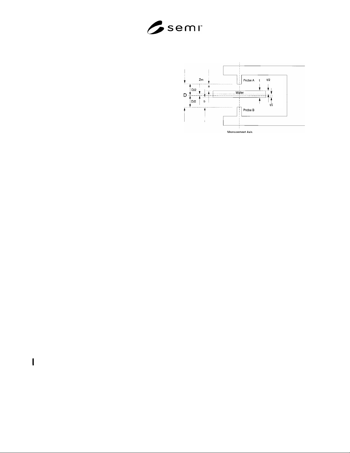
Figure 1
Schematic View of Wafer, Probes, and Fixture
7.1.4.3 Probe assembly with paired non-contacting
displacement-sensing probes, probe supports, and
indicator unit (see Figure 1).
7.1.4.3.1 The probes shall be capable of independent
measurement of the distances a and b between the
probed site on each surface of the sample wafer and the
nearest probe surface.
7.1.4.3.2
The probes shall be mounted above and
below the wafer in a manner so that the probed site on
one surface of the wafer is opposite the probed site on
the other.
7.1.4.3.3 The common axis of these probes is the
measurement axis.
7.1.4.3.4 The probe separation D shall be kept constant
during calibration and measurement.
7.1.4.3.5 Displacement resolution shall be 100 nm or
smaller.
7.1.4.3.6 The probe sensor size shall be 4 mm by 4
mm, or other value to be agreed upon between the
parties to the test.
7.1.4.3.7 Measuring equipment employing either the
Representative Wafer Inversion Method or the Sample
Wafer Inversion Method for gravity compensation must
provide precise positioning in both measurement
orientations so that measurements are taken at identical
locations for each orientation of the sample.
8 Materials
8.1 Set-up Masters — suitable to accomplish
calibration and standardization as recommended by the
equipment manufacturer.
8.2 Reference Wafer — with a reference warp value
20 m that is used to determine the level of agreement

SEMI MF1390-1104 © SEMI 2004 4
between the warp value obtained by the measuring
equipment under test and the reference warp value (see
Section 9).
8.3 Representative Wafer — required only if the
Representative Wafer Inversion Method is used for the
gravity correction. A representative wafer shall be
identical in nominal diameter, nominal thickness,
fiducials, composition and crystalline orientation to
those being measured. Its warp need not be known.
9 Suitability of Measuring Equipment
9.1 Determine the suitability of the measuring
equipment with the use of a reference wafer and its
reference warp value in accordance with the
procedures of Sub-section 9.2, or by performance of a
statistically-based instrument repeatability study to
ascertain whether the equipment is operating within the
manufacturer's stated specification for repeatability.
9.1.1 The reference warp value is the average of a
number of values obtained for that wafer over a number
of “passes” (repeat measurements). The reference
wafer is measured on the measuring equipment under
test and its reference warp value is compared against
the measured warp value. The acceptable level of the
agreement between the reference and measured warp
values is to be agreed upon by the parties to the test.
9.2 Procedure
9.2.1 Select a reference wafer of appropriate criteria,
together with its associated reference warp value.
9.2.2 Measure the reference wafer on the measuring
equipment under test to obtain a sample warp value.
9.2.3 Subtract the two warp values to obtain the
difference:
samplereferencewarp
WarpWarp
(1)
9.2.4 The metric to be used to determine acceptability
is difference,
warp.
Accept the measuring equipment as
suitable for use if this difference is less than a value that
is agreed upon between the parties to the test.
NOTE 4: If the measuring equipment is to be used to
measure other parameters, such as flatness and thickness
variation in addition to warp, the reference and sample warp
values may be included in the reference and sample data sets
specified in SEMI MF1530, but this is not necessary if only
warp measurements are to be made.
10 Sampling
10.1 This test method is nondestructive and may be
used on either 100% of the wafers in a lot or on a
sampling basis.
10.1.1 If samples are to be taken, procedures for
selecting the sample from each lot of wafers to be tested
shall be agreed upon between the parties to the test, as
shall the definition of what constitutes a lot.
11 Calibration and Standardization
11.1 Calibrate the measuring equipment in accordance
with the manufacturer's instructions.
11.2 When using the Representative Wafer Inversion
Method for correcting the gravity-induced deflection,
determine z
gravity
, the deflection due to gravity and
machine effects on the representative wafer, in
accordance with Section 12 and Section 13 through
paragraph 13.7.
12 Procedure
12.1 Prepare the apparatus for measurement of wafers,
including selection of diameter, peripheral fiducials,
scan area and data display/output functions. Also select
the gravitational correction method from one of the
following:
Reference Wafer Inversion Method (see Note 3),
Sample Wafer Inversion Method, or
Theoretical Modeling Method.
12.2 Select the fixed quality area (FQA) by specifying
the nominal edge exclusion (EE).
12.3 Introduce the test specimen into the measurement
mechanism with the front surface upward and initiate
the measurement sequence to determine and record the
distances between each probe and the nearest wafer
surface in pairs, a and b, at each measurement position.
Proceed directly to Section 13 unless (1) the Sample
Wafer Inversion Method is being used to correct for
effects of distortion due to gravity or (2) a
representative wafer is being measured to obtain the
gravity correction for use in the Representative Wafer
Inversion Method (see Note 3).
12.4 Repeat Section 12.2 with the wafer inverted (front
surface downward).
13 Calculations
13.1 The following calculations are performed
automatically within the instrument. An outline of the
calculation structures is provided here to indicate the
nature of the procedure.
13.2 Determine the displacements (distances) between
each probe and the nearest surface of the wafer (in
pairs) at intervals along the scan pattern.