semi合集-English.pdf - 第223页
SEMI E33-94 © SEM I 1994 1 SEMI E33-94 SPECIFIC A TION FOR SEMI CONDUCTOR M ANUFA CTURING F ACILITY ELECTROM A GNETI C COMP ATIBILITY NOTICE: Thi s standard does not purport to address safety problems associated with its…

SEMI E31-93 © SEMI 1993 4
NOTICE: These standards do not purport to address
safety issues, if any, associated with their use. It is the
responsibility of the user of these standards to establish
appropriate safety and health practices and determine
the applicability of regulatory limitations prior to use.
SEMI makes no warranties or representations as to the
suitability of the standards set forth herein for any
particular application. The determination of the
suitability of the standard is solely the responsibility of
the user. Users are cautioned to refer to manufacturer’s
instructions, product labels, product data sheets, and
other relevant literature respecting any materials
mentioned herein. These standards are subject to
change without notice.
The user’s attention is called to the possibility that
compliance with this standard may require use of
copyrighted material or of an invention covered by
patent rights. By publication of this standard, SEMI
takes no position respecting the validity of any patent
rights or copyrights asserted in connection with any
item mentioned in this standard. Users of this standard
are expressly advised that determination of any such
patent rights or copyrights, and the risk of infringement
of such rights, are entirely their own responsibility.
Copyright by SEMI® (Semiconductor Equipment and Materials
International), 3081 Zanker Road, San Jose, CA 95134. Reproduction o
f
the contents in whole or in part is forbidden without express written
consent of SEMI.

SEMI E33-94 © SEMI 19941
SEMI E33-94
SPECIFICATION FOR SEMICONDUCTOR MANUFACTURING FACILITY
ELECTROMAGNETIC COMPATIBILITY
NOTICE: This standard does not purport to address
safety problems associated with its use. It is the
responsibility of the user of this standard to establish
appropriate safety and health practices and determine
the applicability of regulatory limitations prior to the
use.
1 Introduction
1.1 Purpose — The purpose of thi s specification is to
assure that semiconductor manufacturing facilities and
the equipment used for manufacturing semiconductor
devices will operate together reliably without failures
caused by electromagnetic interference or electrostatic
discharge. This goal is generally known as
“electromagnetic compatibility” or EMC.
1.2 Scope — This specification app lies to facilities
and equipment constructed for the purpose of
manufacturing semiconductor devices including all
facilities alarm, safety, communications and control
systems, processing equipment, metrology equipment,
automation equipment, and information technology
equipment.
1.3 Limitations — This specification does not apply to
the equipment and facilities used for the assembly and
functional testing of integrated circuits. This
specification does not apply to process-specific
charging that may occur to semiconductors under
manufacture.
2 Referenced Documents
2.1 ANSI, C63.4-1991
1
— America n National
Standard for Methods of Measurement of Radio-Noise
Emissions from Low-Voltage Electrical and Electronic
Equipment in the Range of 9 kHz to 40 GHz
2.2 CISPR, Publication 22, 19852
2
— Limits and
Methods of Measurement of Radio Interference
Characteristics of Information Technology Equipment
2.3 CENELEC, EN 55 022, 1987
2
— Modifications to
CISPR 22
1 IEEE Service Center, 445 Hoes Lane, P.O. Box 1331, Piscataway,
NJ 08855.
2 Sales Department of the Central Office of the IEC, P.O. Box 131, 3,
Rue de Varembe, 1121 Geneva 20, Switzerland. Some of the IEC
publications are available from the Sales Department, American
National Standards Institute, 11 W. 42nd Street, New York, NY
10036.
Draft British Standard EN 50 082-2
3
—
Electromagnetic Compatibility — Generic Immunity
Standard: Industrial (CLC/TC 110 (Sec) 44)
2.4 Emerald Book
1
— IEEE Reco mmended Practice
for Powering and Grounding Sensitive Electronic
Equipment, IEEE, 1992
2.5 EOS/ESD Association Advisory for Electrostatic
Discharge Terminology
4
— Glossary, 1992
2.6 FIPS (Federal Information Processing Standards)
Publication 94, 21 September 1983
5
— Guideline on
Electrical Power for ADP Installations
2.7 IEC 801-2, Second Edition, 1991-04
2
—
Electrostatic Discharge Requirements
2.8 IEC 801-3, First Edition, 1984
2
— Radiated
Electromagnetic Field Requirements
2.9 IEC 801-4, First Edition, 1988
2
— Electrical Fast
Transient/Burst Requirements
2.10 IEC TC 65 (Sec.) 137 (801-5) Committee Draft,
July 1992
2
— Surge Immunity Requirements
2.11 IEC TC 65 (Sec.) 144 (801-6) Committee Draft,
February 1992
2
— Immunity to Conducted
Disturbances Induced by Radio Frequency Fields above
9 kHz.
3 Terminology
3.1 earth port — European term fo r an equipment
ground. This term is used extensively in the basic
standards.
3.2 electromagnetic compatibility (EMC) — The
ability of electronic equipment to function properly
with respect to environmental EMI and ESD.
3.3 electromagnetic interference (EMI) — Any
electrical signal in the non-ionizing (sub-optical)
portion of the electromagnetic spectrum with the
potential to cause an undesired response in electronic
equipment.
3 Sales Administration (Drafts), BSI, Linford Wood, Milton Keynes
MK 14 6LE, United Kingdom.
4 EOS/ESD Association, Inc., 200 Liberty Plaza, Rome, NY 13440.
5 National Technical Information Service, U.S. Department of
Commerce, Springfield, VA 22161.
SEMI E33-94 © SEMI 1994 2
3.4 electrostatic discharge (ESD) — The transfer of
electrostatic charge between bodies at different
electrostatic potentials.
3.5 ELF — Extremely low frequen cy (about 1 Hz to 1
kHz) magnetic fields generated by current flow (most
commonly 60 Hz in the U.S. and 50 Hz in Europe)
within equipment and facilities.
3.6 ELF sensitive equipment — Any equipment whose
performance is adversely affected by ELF, such as a
scanning electron microscope (SEM).
3.7 EUT — Equipment under test.
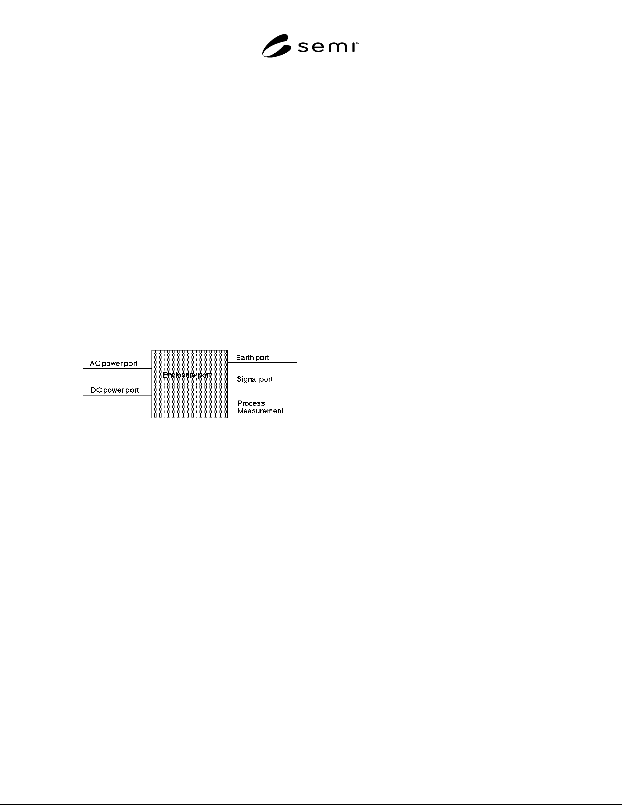
3.8 port — (For purposes of this specification), a
particular interface of the specified equipment with the
external electromagnetic environment, (see Figure 1).
3.9 enclosure port — (For purpose s of this
specification), the physical boundary of the apparatus
through which electromagnetic fields may radiate or
impinge.
Figure 1
4 Requirements
4.1 Performance Criteria — The following are
generic failure criteria for the various classes of
equipment and electronic systems used in
semiconductor manufacturing. However, any kind of
failure or aberration during EMC testing shall be noted
in the test report.
4.1.1 Performance Criteria A — The equipment
operates as intended during and after the test. In the
case of process equipment, all process results are within
specifications. No safety hazards nor false alarms are
present. In some cases, the performance level may be
replaced by a documented permissible loss of
performance if such loss is minor and agreeable to the
concerned parties.
4.1.2 Performance Criteria B — The equipment
operates as intended after the test, but experiences a
loss of function or degradation of performance during
the test to a level specified by the manufacturer. No
change of operating state or loss of stored data is
allowed. Restoration of performance or function does
not require human intervention.
4.1.3 Performance Criteria C — Te mporary loss of
function is allowed, provided the loss of function is
recoverable, either automatically or through operation
of the controls. Any failure of control or alarm systems
is in a fail-safe mode, such as a false alarm or
equipment shutdown.
4.1.4 Safety Criteria — Equipment will automatically
fail if testing results in an unsafe or potentially unsafe
condition, such as threat to life or property. Examples
would be failure of an emergency machine off (EMO)
button to operate or faulty opening of a toxic gas valve.
4.1.5 Conditions during Testing — All EMC testing is
to be done with the equipment installed and operational.
As much as possible, the test installation should be
identical to the final production installation. Substitutes
may be used for hazardous gases and chemicals, and
other modifications may be made as deemed reasonable
to ensure testing can be performed in a completely safe
and environmentally acceptable manner. Special EMC
facilities are not required by this standard.
5 Test Methods
The tables below are organized by ports to which the
tests apply, as defined above. The basic standards
provide the test setup and procedures to be followed,
except as noted. In all events, EMC testing is intended
to prevent EMC problems when the equipment is
installed and operating in a semiconductor
manufacturing facility. Any modification or
interpretation of the test setup and procedure should be
judged by this overriding goal.