semi合集-English.pdf - 第5226页
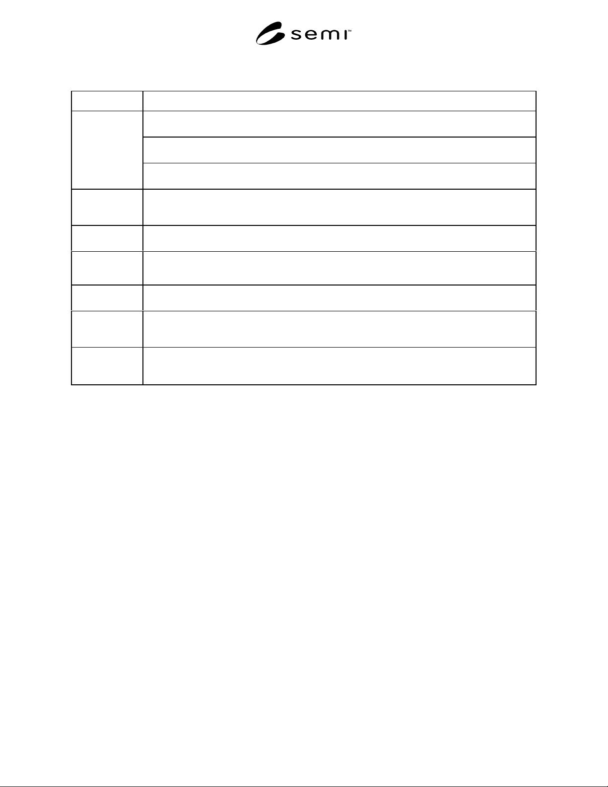
SEMI M40-0200 © SE MI 2000 8 Table 1 Roughness Measurement Codes Element Abbrevia tion Item A1 2 3 4 Profilom eter AFM SPM OPR MPR B1 Interferometer IM C1 2 3 Instrument Scatterometer TIS ARLS SSIS 15 9 R C S Pattern (Se…

SEMI M40-0200 © SEMI 20007
9.2.1.1 Interferometer
a. Interference microscope
9.2.1.2
Profilometer
a. AFM
b. Other scanning probe microscopes
c. Optical profilometer
d. Mechanical stylus
9.2.1.3
Scatterometer
a. Total Integrating (TIS)
b. Angle-resolved light (ARLS)
c. Scanning Surface Inspection System (SSIS)
9.3
Next, select the roughness para meter to by
calculated.
9.4 Select the measurement pattern (Figure 1):
a. Center point
b. 5-point
c. 9-point
d. Full-FQA raster scan
e. Full-FQA R-theta scan
9.5
Select the pattern orientation ( Figure 1)
a. Type A
b. Type B
9.6
Select the local measuring condition
a. Point
b. Line
c. Area
9.7
Specify the measurement calculations to be
reported
a. Average (A)
b. Range (R)
c. Maximum (M)
d. Standard Deviation, 1 sigma (S
n-1
)
9.8 Specify the bandwidth and sca n length limits
within which data is to be gathered.
9.9 Lastly, record the abbreviations describing these
selections (see Appendix 1 for examples), separating
adjacent abbreviations with a comma and using periods
for decimal notation. This creates a seven-field
abbreviation. The field sequence described above
follows the order of elements in Table 1.
10 Measurement Reporting S equence
10.1 In general, one value is reported for a wafer.
Where more than one pattern is specified the calculated
values are reported in the order in which they are listed
in Table 1.
SEMI M40-0200 © SEMI 2000 8
Table 1 Roughness Measurement Codes
Element Abbreviation Item
A12 3 4
Profilometer AFM SPM OPR MPR
B1
Interferometer IM
C12 3
Instrument
Scatterometer TIS ARLS SSIS
159 R C SPattern
(See NOTE 1.)
Center 5-point 9-point FQA/Raster
scan
FQA/Concentric
R-theta scan
FQA/Spiral
R-theta scan
ABPattern
Orientation
AB
PLALocal
Measurement
Condition
Point Line Area
QAZ TKSParameter
(See NOTE 1.)
Rq Ra Rz Rt Kurtosis Skewness
ARM DCalculation
(See NOTE 1.)
Average Range Maximum Std. Deviation
(1 sigma
n-1
)
Bandwidth, µm [ __ ]/[ __ ]
(fill in blanks to two significant figures)
Long wavelength (µm)/Short wavelength (µm)
NOTE 1: If more than 1 element is specified, the representative letters are concatenated in the relevant field, in the order specified. See Appendix
1 for examples.
SEMI M40-0200 © SEMI 20009
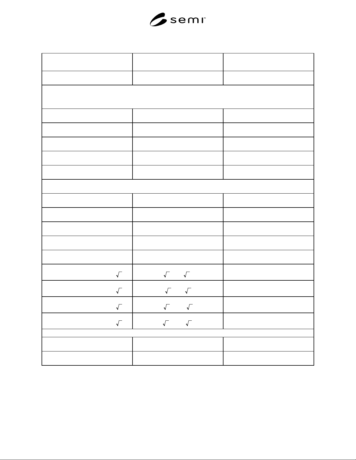
Table 2 Scan Pattern Locations
Location X, Y Coordinates
(per SEMI M20)
Scan Direction (for line and area
tools), parallel to:
Center Point 0, 0 Y-axis
5-point Pattern
Point # Location
1 Center Point 0, 0 Y-axis
2 2r/3 0, 2r/3 Y-axis
3 2r/3 -2r/3, 0 X-axis
4 2r/3 0, -2r/3 Y-axis
5 2r/3 2r/3, 0 X-axis
9-point Pattern
1Center0, 0 Y-axis
2 4r/5 0, 4r/5 Y-axis
3 4r/5 -4r/5, 0 X-axis
4 4r/5 0, -4r/5 Y-axis
5 4r/5 4r/5, 0 X-axis
6(r2 )/5 (r 2 )/5, (r 2 )/5
Y-axis
7(r2 )/5 - (r 2 )/5, (r 2 )/5
X-axis
8(r2 )/5 - (r 2 )/5, - (r 2 )/5
Y-axis
9(r2 )/5 (r 2 )/5, - (r 2 )/5
X-axis
Full FQA Scan
Raster Scan Full FQA X-axis
Concentric Circles or Spiral Full FQA
R – Theta
NOTE 1: r = nominal wafer radius