semi合集-English.pdf - 第6155页
SEMI G32-94 © SEMI 198 6, 1994 4 Figure 2 Pictorial Representation of Scaled Test Chip NOTICE: T hese st andards do not pu rport to address s afety issues, if any, associated with their use. It is the responsibility of t…
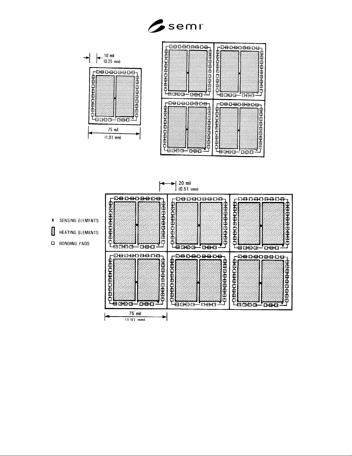
SEMI G32-94 © SEMI 1986, 19943
Figure 1
Pictorial Representation of Arrayed Thermal Test Chip
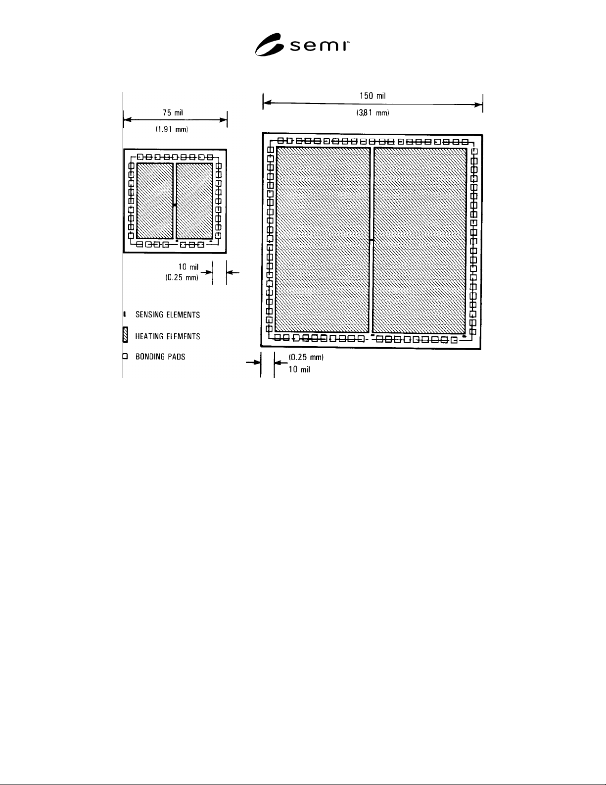
SEMI G32-94 © SEMI 1986, 1994 4
Figure 2
Pictorial Representation of Scaled Test Chip
NOTICE: These standards do not purport to address safety issues, if any, associated with their use. It is the
responsibility of the user of these standards to establish appropriate safety and health practices and determine the
applicability of regulatory limitations prior to use. SEMI makes no warranties or representations as to the suitability
of the standards set forth herein for any particular application. The determination of the suitability of the standard is
solely the responsibility of the user. Users are cautioned to refer to manufacturer’s instructions, product labels,
product data sheets, and other relevant literature respecting any materials mentioned herein. These standards are
subject to change without notice.
The user’s attention is called to the possibility that compliance with this standard may require use of copyrighted
material or of an invention covered by patent rights. By publication of this standard, SEMI takes no position
respecting the validity of any patent rights or copyrights asserted in connection with any item mentioned in this
standard. Users of this standard are expressly advised that determination of any such patent rights or copyrights, and
the risk of infringement of such rights, are entirely their own responsibility.
Copyright by SEMI® (Semiconductor Equipment and Materials
International), 3081 Zanker Road, San Jose, CA 95134. Reproduction o
f
the contents in whole or in part is forbidden without express written
consent of SEMI.

SEMI G33-90 © SEMI 1986, 19961
SEMI G33-90
SPECIFICATION FOR PRESSED CERAMIC PIN GRID ARRAY
PACKAGES
1 Preface
This specification defines the acceptance criteria for
ceramic pin grid array packages produced using pressed
ceramic, mechanically inserted pins and solder for
electrical interconnection of pins.
2 Applicable Documents
2.1 ANSI Specification
1
Y14.5 — Dimensioning and Tolerancing
2.2 ASTM Specification
2
B 152 — Copper Metal Specification
2.3 Federal Specification
3
QQ-N-290A — Nickel Plating
QQ-S-571E — Solder-Alloy Compositions
2.4 Military Specifications
3
MIL-STD-105 — Sampling Procedures and Tables for
Inspection by Attributes
MIL-STD-883 — Test Methods and Procedures for
Microelectronics
MIL-G-45204 — Gold Plating, Electrodeposited
MIL-M-38510 — General Specification for
Microcircuits
2.5 JEDEC Specification
4
Pub. No. 95 — Registered and Standard Outlines for
Semiconductor Devices
3 Selected Definitions
blister (bubble) ceramic — Any separation within the
ceramic which does not expose underlying ceramic
material.
blister (bubble) metal — Any localized separation
within the metallization or between the metallization
and ceramic which does not expose underlying
metallization or ceramic material.
1 ANSI, 1430 Broadway, New York, NY 10018
2 American Society of Testing and Materials, 100 Barr Harbor Drive,
West Conshohoken, PA 19428-2959
3 Military Standards, Naval Publications and Form Center, 5801
Tabor Avenue, Philadelphia, PA 19120
4 JEDEC, 2001 Eye Street N.W., Washington, D.C. 20006
burr — An adherent fragment of excess parent material
at the component edge.
chip — A region of ceramic missing from the surface or
edge of a package which does not go completely
through the package. Chip size is given by its length,
width and depth from a projection of design planform
(see Figure 1).
crack — A cleavage or fracture that extends to the
surface of a package which may or may not pass
through the entire thickness of the package.
contact pad — That metallized pattern that provides
mechanical or electrical connection to the external
circuitry.
die attach surface — A dimensional outline designated
for die attach.
dielectric — A material applied to the surface of a
package which provides such functions as electrical
insulation, passivation of underlying metallization and
limitation of solder flow.
discoloration — Any change in the color of the
package metallization as detected by the unaided eye.
flatness — The allowable deviation of a surface from a
reference plane. The tolerance zone is defined by two
parallel planes within which the surface must lie.
footprint — Pin pattern.
foreign material — An adherent particle other than
parent material.
isolation gap — Metal-free space between conductive
areas.
peeling (flaking) — Any separation of metallization
from the base material exposing the base material.
pit — Any unspecified depression in the package.
post-metallization — The process by which
metallization is applied to a body (substrate) after the
body has been fully sintered.
projection — An adherent fragment of parent material
on the package surface.
pullback — The linear distance between the edge of the
ceramic and the first measurable metallization and/or
glass interface (see Figure 2).
refractory metallization — The process by which a high
melting point (typically in excess of 1800°C) metal or