semi合集-English.pdf - 第4608页
SEMI D40-0704 © SEMI 2004 2 Sag Substrate Support Plai n Bevele d regi on A Figure 3 Definition of Sa g at Edge NOTE 2: In case there is lift a t the edge of a substrate, lift is defined by the distance to positio n “B” …
SEMI D40-0704 © SEMI 2004 1
SEMI D40-0704
TERMINOLOGY FOR FPD SUBSTRATE DEFLECTION
This standard was technically approved by the Global Flat Panel Display - Factory Automation Committee
and is the direct responsibility of the Japanese Flat Panel Display - Factory Automation Committee. Current
edition approved by the Japanese Regional Standards Committee on April 30, 2004. Initially available at
www.semi.org June 2004; to be published July 2004.
1 Purpose
1.1 This document provides the terms and definitions
of a physical transformation when flat panel display
(FPD) substrates are maintained statically.
2 Scope
2.1 These terms and definitions are applicable to both
front and back substrates used in FPD fabrication.
NOTICE: This standard does not purport to address
safety issues, if any, associated with its use. It is the
responsibility of the users of this standard to establish
appropriate safety and health practices and determine
the applicability of regulatory or other limitations prior
to use.
3 Limitations
3.1 This standard is not applicable to sag at
transportation between substrate venders and FPD
manufacturers.
4 Referenced Standards
4.1 SEMI Standards
SEMI D9 Terminology For FPD Substrates
SEMI D25 Specification For Flat Panel Display
Substrate Shipping Case
NOTICE: Unless otherwise indicated, all documents
cited shall be the latest published versions.
5 Terminology
5.1 Definitions
5.1.1 Displacement Terminology — The displacement
is generated by sag and lift caused by the supporting
positions and/or locations of the FPD substrate. The
displacement is defined by the values of two-
dimensional sag and lift. Two dimensional maximum
displacement is also defined by values of two-
dimensional maximum sag and lift, and the thickness of
the FPD substrate.
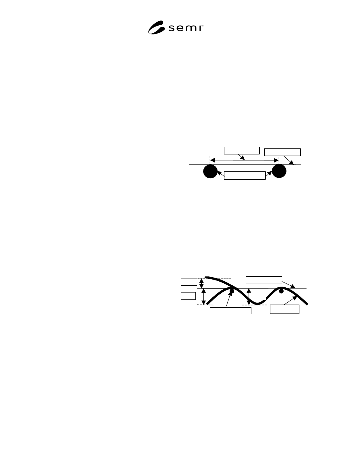
5.1.1.1 support plain — a support plain is defined as a
horizontally ideal flat plain which is enhanced from a
horizontally straight line defined from the top position
of the support members, as shown in Figure 1.
5.1.1.2 support member support member is a
support device such as a support pin to support FPD
substrates, as shown in Figure 1.
5.1.1.3 support span support span is defined as at
least the distance between two support members, as
shown in Figure 1.
Support Member
Support plain
Support Span
Figure 1
Definitions of Support Span, Support Member and
Support Plain
5.1.1.4 lift lift is defined as the displacement to the
bottom surface of substrate from the support plain. It is
located above position from the support plain, as shown
in Figure 2.
5.1.1.5 sag sag is defined as the generated distance
between the bottom surface of the substrate and the
support plain caused by gravity, as shown in Figure 2.
Substrate
Support Plain
Support Member
Lift
Sag
Sag
Figure 2
Definitions of Lift and Sag
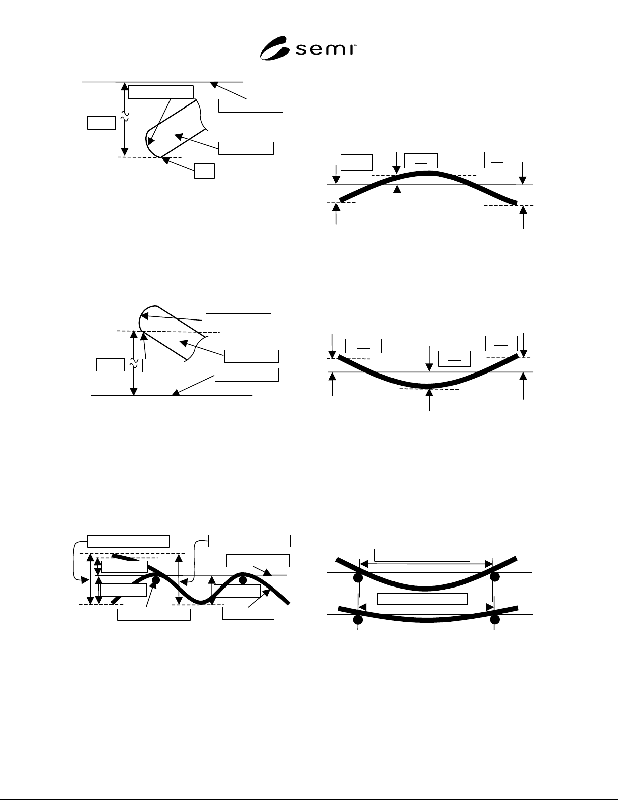
NOTE 1: In case there is sag at the edge of a substrate, sag is
defined by the distance to position “A” from the support
plain. The position “A” is determined by the intersection point
of between the edge of the bottom surface of the substrate and
the edge of the beveled region, as shown in Figure 3.
SEMI D40-0704 © SEMI 2004 2
Sag
Substrate
Support Plain
Beveled region
A
Figure 3
Definition of Sag at Edge
NOTE 2: In case there is lift at the edge of a substrate, lift is
defined by the distance to position “B” from the support plain.
The position “B” is determined by the intersection point of
between the edge of the bottom surface of the substrate and
the edge of the beveled region, as shown in Figure 4.
Lift
Substrate
Support Plain
Beveled region
B
Figure 4
Definition of Lift at Edge
5.1.1.6 maximum displacement two-dimensional
maximum displacement (Max. Displacement) is defined
by maximum lift (Max. Lift) + maximum sag (Max.
Sag) + substrate thickness. Maximum displacement can
have the same value at several different locations, as
shown in Figure 5.
Max. Sag
Substrate
Support plain
Support Member
Max. Lift
Max. Sag
Max. Displacement
Max. Displacement
Figure 5
Maximum Displacement
5.1.2 Displacement Mode Terminology
displacement modes are classified into five types
caused by supporting conditions, which are number of
supporting positions, distance of each supporting
position and location of supporting positions.
5.1.2.1 A Type substrates of this type have a convex
shape. The substrate shape is named “A type”. A type
mode consists of lift at center location and two sags at
the left and right edges, as shown in Figure 6.
Lift
Sag
Sag
Figure 6
A Type Substrate Shape
5.1.2.2 U Type the type is the concave shape of
substrate. The substrate shape is named as “U type”. U
type mode consists of Sag at center location and two
lifts which are consist of the Lift at left and at right
edge locations, as shown in Figure 7.
Lift
Sag
Lift
Figure 7
U Type Substrate Shape
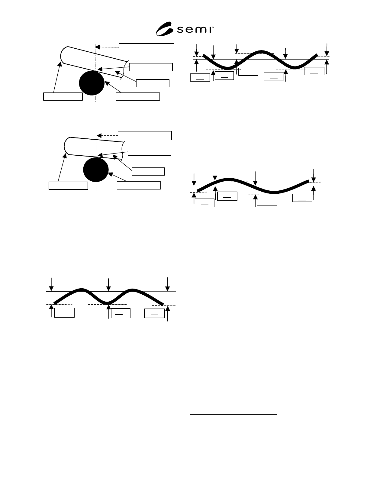
NOTE 3: Depending on conditions, support span length may
change slightly due to the substrate slipping on its support
members, as shown in Figure 8. The support span is shorter
when sag is relatively larger, as shown in Figure 9. On the
other hand, the support span is longer when sag is relatively
smaller, as shown in Figure 10. Since the change of support
span is predicted to be significantly smaller than the support
span, the change of support span is ignored.
Shorter support span
Longer support span
Figure 8
Change of Support Span Due to Sag Magnitude
SEMI D40-0704 © SEMI 2004 3
Substrate
Support Member
Beveled region
Support Position
Shorter Support Span
Figure 9
Position on Small Sag
Substrate
Support Member
Beveled region
Support Position
Longer Support Span
Figure 10
Position on Large sag
5.1.2.3 M Type the type has an alphabetic “M”
shape, which mixes the convex shape and the concave
shape, as shown in Figure 11. This substrate shape is
named “M type”. M type consists of all sag and
requires sag to exist at both edge regions of the
substrate, even if the substrate has a continuous wave or
corrugation in its shape.
Sag
Sag
Sag
Figure 11
M Type Substrate Shape
5.1.2.4 W Type the type has an alphabetic “W”
shape, which mixes the convex shape and the concave
shape, as shown in Figure 12. This substrate shape is
named “W” type. W type combines sag and lift. Also W
type requires lift to exist at both edge regions of the
substrate, even if the substrate has a continuous wave or
corrugation in its shape.
Lift
Lift
Lift
Sag
Sag
Figure 12
W Type Substrate Shape
5.1.2.5 S Type the type has a rotated alphabetic “S”
shape, which mixes the convex shape and the concave
shape, as shown in Figure 13. This substrate is named
“S” type. S type combines sag and lift. Also S type
requires an asymmetrical shape, which consists of sag
and lift at both edge regions, even if the substrate has a
continuous wave or corrugation in its shape.
Sag
Lift
Sag
Lift
Figure 13
S Type Substrate Shape
6 Related Documents
6.1 SEAJ
1
(Semiconductor Equipment Association of
Japan) Liquid Crystal Display Manufacturing
Equipment Dictionary
NOTICE: SEMI makes no warranties or
representations as to the suitability of the standards set
forth herein for any particular application. The
determination of the suitability of the standard is solely
the responsibility of the user. Users are cautioned to
refer to manufacturer' s instructions, product labels,
product data sheets, and other relevant literature,
respecting any materials or equipment mentioned
herein. These standards are subject to change without
notice.
By publication of this standard, Semiconductor
Equipment and Materials International (SEMI) takes no
position respecting the validity of any patent rights or
copyrights asserted in connection with any items
mentioned in this standard. Users of this standard are
expressly advised that determination of any such patent
rights or copyrights, and the risk of infringement of
such rights are entirely their own responsibility.
1 Semiconductor Equipment Association of Japan, 4F Grand Maison
Shinjuku Gyoen., 1-7-10 Shinjuku Shinjuku-ku, Tokyo 160-0022
Japan Phone 03.3353.7651 Fax 03.3353.7970
Copyright by SEMI® (Semiconductor Equipment and Materials
International), 3081 Zanker Road, San Jose, CA 95134. Reproduction o
f
the contents in whole or in part is forbidden without express written
consent of SEMI.