semi合集-English.pdf - 第4548页
SEMI D26-1000 © SEM I 2000 7 7.7 Edge L ength and Thicknes s — T h e se d imensi ons apply to photom a sks th a t are principally used in fabricating flat panel display. The edge lengths specifi ed range from 202.8 mm × …
SEMI D26-1000 © SEMI 2000 6
after attachment. No part of the frame adhesive may
extend beyond the frame wall, and its edges must be
free of visually detectable stringers (and particles).
Adhesive should form a complete seal between the
frame and the mask over a minimum of 40% of the
width of the frame.
7.6.2.2 Frame — Pellicle frame must have no visually
detectable machining burrs, discontinuities in
anodization, or particles.
7.6.2.3 Light Resistance — This is expressed by total
exposure energy value (mJ/cm
2
or J/cm
2
) on pellicle
film resulting in a 1% loss of transmission at any
wavelength in the range 360 nm–440 nm. Also the test
conditions (special characteristics of exposure wave-
length, exposure energy between 360 nm–440 nm,
exposure conditions, and others) must be clearly stated.
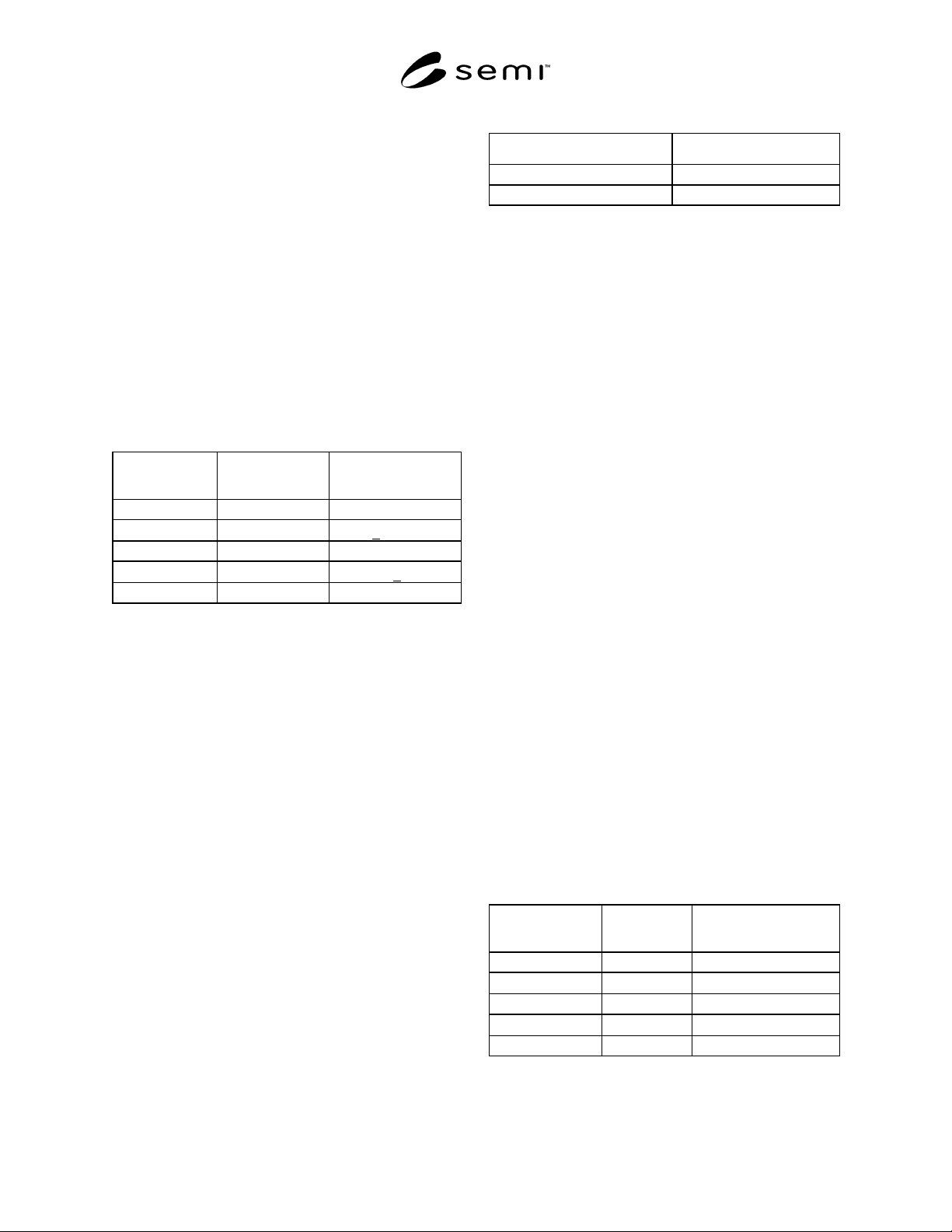
Table 2 Maximum Defect Limits
Characteristics Max. # Allowable Size counted for Max.
# Allowable
Non-removable
Particles None
> 50 µm
Pinholes None > limit of detection
Scratches None
Width > 50 µm
Dirt None > limit of detection
7.6.3 Pellicles for g, h and i Exposure Systems — This
specification includes the characteristics of pellicles for
use in "g" (436 nm), "h" (405 nm), and "i" (365 nm)
line exposure systems.
7.6.3.1 Shape, Size, and Standoff of Pellicle
7.6.3.1.1 Shape — This is determined by agreement
between the user and supplier.
7.6.3.1.2 Size — This is determined by agreement
between the user and supplier, but expression of
tolerance is as follows:
• Outer diameter tolerance: +0, -x
• Inner diameter tolerance: +x, -0
7.6.3.1.3 Standoff — 6.3 mm and 4.0 mm should be
standard.
7.6.3.1.3.1 Tolerance — + 0, -x
7.6.3.2 Film Characteristics Polymer Films — Type:
AR-coated or non AR-coated.
7.6.3.3 Exposure Wavelength — "g", "h", and/or "i"
lines.
7.6.3.4 Optical Transmission Rate — There are the
following two types depending on optical transmission
rate at incident angle of 90° from surface of pellicle at
the specified wavelength(s).
Table 3 Film Characteristics Polymer Films
Type Minimum
AR Coated 99 %
Non AR Coated 98 %
7.6.3.5 Thickness — This is determined by agreement
between the user and supplier.
7.6.3.6 Thickness Conformity — This is determined by
agreement between the user and supplier.
7.6.3.7 Thickness Uniformity — This is determined by
agreement between the user and supplier.
7.6.3.8 Film Thickness — This is determined by
agreement between the user and supplier.
7.6.3.9 Mechanical Strength — The requirements for
air blow are determined within ranges shown below:
7.6.3.9.1 The air blow gun should be used. Air
pressure: ≤ 2.1 kgf/cm
2
(at input of the air blow gun).
Nozzle diameter of the air blow gun: ≤ 2 mm.
7.6.3.9.2 Distance between the nozzle tip and the film:
≥ 25 mm.
7.6.3.10 Defect Limits — Maximum defect limits
based on the pellicle standoff and the numerical
aperture of the given type of exposure system are given
in Table 4. Any departure from these defect limits shall
be agreed to between the user and supplier.
7.6.3.11 Frame — Pellicle frame must have no
visually detectable machining burrs, discontinuities in
anodization, or particles.
7.6.3.12 Light Resistance — This is expressed by total
exposure energy value (mJ/cm
2
or J/cm
2
) of specified
wavelength on pellicle film resulting in a 0.5% loss of
transmission at any wavelength in the range 360–440
nm. Also, the test conditions (half bandwidth of
exposure specified wavelength, energy of exposure
specified wavelength, exposure conditions, and others)
must be clearly specified.
Table 4 Maximum Defect Limits
Characteristics Max. No.
Allowable
Size Counted for Max.
No. Allowable
Non-removable
Particles None
> 20 µm
Pinholes None > limit of detection
Scratches None
Width > 20 µm
Dirt None > limit of detection
SEMI D26-1000 © SEMI 20007
7.7 Edge Length and Thickness — These dimensions
apply to photomasks that are principally used in
fabricating flat panel display. The edge lengths
specified range from 202.8 mm × 202.8 mm to 620 mm
× 720 mm. Substrates with an edge length less than 200
mm follow the specification for a semiconductor mask
(see SEMI P1and SEMI D6).
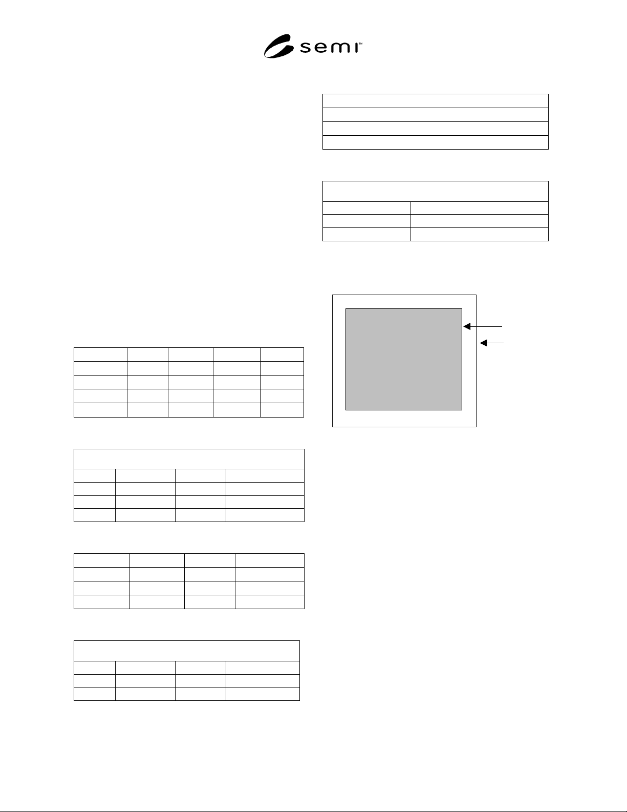
7.7.1 Edge Length and Tolerance — Units are in mm.
See Table A1 and A2 and Table B1 and B2 and Table
C1 and C2 for a combination of materials, edge length,
and thickness.
7.7.1.1 Edge Length Tolerance — + 0.4 mm. Applies
to all groups.
7.7.2 Thickness Center Point — Thickness of
substrates at center point shall be specified by the edge
length group and materials as shown in Tables A2, B2
and C2.
7.7.2.1 Tolerance — ≤ 5 mm ± 0.2 mm, 8 mm + 0.2
mm, - 0.4 mm.
Table A-1 Edge Length (mm) (Group A)
202.8 × 202.8
200 × 250 250 × 250
250 × 300 300 × 300
300 × 350 350 × 350
350 × 400 400 × 400
Table B-1 Plate Thickness and Materials (Group A)
MATERIAL
HTE MTE/LTE ULTE Thickness (mm)
++ + 3.0
+4.8
++ 5.0
Table A-2 Edge Length (mm) (Group B)
330 × 450
400 × 500
450 ×550
500 × 600
Table B-2 Plate Thickness and Materials (Group B)
MATERIAL
HTE MTE/LTE ULTE Thickness (mm)
+4.8
++ + 5.0
Table C-1 Edge Length (Group C)
620 × 720 mm
650 × 750 mm
650 × 800 mm
700 × 800 mm
Table C-2 Plate Thickness and Materials (Group C)
MATERIAL
ULTE Thickness (mm)
+5.0
+8.0
7.7.2.2 The active area is defined as area within the
plate that is within 20 mm from the edge of the plate
(See Figure 5).
20 mm minimum
Active
Area
Figure 5
Defined Active Area
7.8 Data Formats
7.8.1 Data Transfer Standards — CAD data for mask
generation can be designed with and delivered to the
vendor in several different standardized data transfer
formats. Among these are DXF, Gerber and its variants
(274-D, 274-X, F9XXX, and BARCO DPF), GDSII,
EDIF, IGES, and IPC-D-350.
7.8.2 Non-Recommended Practices — The following
is a summary of some design practices and CAD
entities that should be avoided when using DXF and
Gerber data formats, since their use can have at best
unintended results.
7.8.2.1 DXF
• Commands regarding 3D CAD.
• Parameters which control the view only, such as
3DFACE, VIEWPORT, STYLE, VIEW,
DIMSTYLE, UCS, APPID, ATTRIB, ATTDEF,
and POINT
• HATCH
SEMI D26-1000 © SEMI 2000 8
• Outlines constructed with ARC and LINE that do
not match exactly at the corners
• Duplicated entities
• Self-intersecting poly-lines
• VERTEX flags options
• TAPERED POLYLINE entities (different start and
end width), straight or arced
• SHAPE entities
• ELLIPSE entities
• "Stretched” BLOCK entities – blocks with
different X- and Y-scale factor
• Rotated BLOCK entities
• POINT entities
• Any of the "Curve-fitted" POLYLINE entities,
such as "SPLINE" shapes
• “Paint & Scratch” LAYER entities without a
specific identification of which layers should be
opaque and which should be clear, and in which
order.
• TEXT entities without the appropriate font files.
• TEXT entities with special attributes (mirror,
rotate, slant, etc.).
• XREF BLOCK entities.
• Non-decimal linear and angular coordinates.
• Radian angular units.
7.8.2.2 Gerber
• Self-intersecting entities (line draws, outlines,
“butterfly targets”, etc.).
• Arrayed arrays (nested).
• Drawn apertures using shapes other than round
(square apertures may be used only if drawn
parallel to either axis).
7.8.3 Recommended Practices — The following is a
summary of some recommended design practices DXF
and Gerber data formats.
7.8.3.1 DXF
• SOLID entities
• TRACE entities
• CIRCLE entities
• BLOCKS, with a minimum level of nesting as
required by the design
• Closed, zero width POLYLINE or LWPOLYLINE
entities to describe complex CAD feature outlines
• TEXT objects that are exploded and exported as
POLYLINE entities, either as closed zero width, or
POLYLINE entities with width
• Decimal units for inches, mils, millimeters,
microns, or degrees.
7.8.4 Gerber
• Subfigure or SR codes.
• POEX/POIN or G36/G37 codes.
• Complex apertures and aperture macros.
• Embedded apertures and parameters.
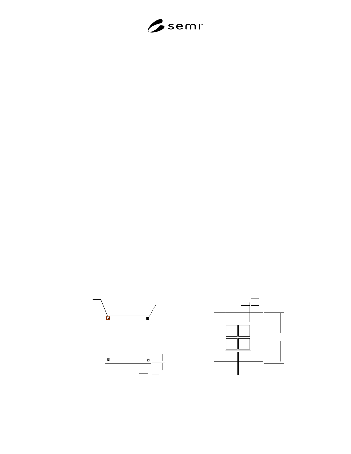
40 um
40 um
1500 um
800 um
10 mm
10 mm
Target
Photomask
4X Targets
200um borde
r
around this
target
Figure 6
Location and Pattern