semi合集-English.pdf - 第7346页
SEMI MF1390-1104 © SEMI 2004 6 13.13.1 Record sample st andard de viation and other statistical parameters as agreed upon between the parties to the test. 14 Report 14.1 Report the following information: 14.1.1 Date, tim…

SEMI MF1390-1104 © SEMI 2004 5
NOTE 5: From Figure 1, note that the distance between
Probe A and the nearest surface of the wafer is displacement
value a and the distance between Probe B and the nearest
surface of the wafer is displacement value b.
13.3 Set the origin of the z-axis at the midpoint between
the two probes, A and B.
13.4 Find the distance, z
m
, of the median surface from
the z-axis origin at each point. From Figure 1,
22
t
a
D
z
m
(2)
and
22
t
b
D
z
m
(3)
Therefore,
m
z
t
b
Dt
a
D
2
2222
(4)
and
2
ab
z
m
(5)
where
D = distance between Probes A and B,
a = distance between Probe A and the nearest
(top) wafer surface,
b = distance between Probe B and the nearest
(bottom) wafer surface, and
t = wafer thickness.
13.5 For measurements in the normal orientation (front
surface up), call the position of the median surface z
nor
.
13.6 For measurements in the inverse orientation (back
surface up), call the position of the median surface z
inv
.
13.7 For measurements on representative wafers or on
sample wafers when the Sample Wafer Inversion
Method is being used, determine the gravitational
correction to the median surface as follows:
2
invnor
gravity
zz
z
(6)
NOTE 6: This cancels the effect of the representative wafer's
shape while retaining the effect of gravity.
13.8 Determine the gravity compensated median sur-
face as follows:
13.8.1 Representative Wafer Inversion Method —
Subtract z
gravity
from z
nor
to produce z
com
at each
measurement point.
NOTE 7: The Representative Wafer Inversion Method deals
not only with first-order gravitational effects, but also with
other effects that may influence the measured value, such as
wafer-periphery effects, some machine-specific signature, etc.
13.8.2 Sample Wafer Inversion Method — Subtract
z
gravity
from z
nor
to produce z
com
at each measurement
point. Note that this is equivalent to taking the
difference between the normal and inverted
measurement values at each point:
22
invnorinvnor
norgravitynorcom
zzzz
zzzz
(7)
13.8.3 Theoretical Modeling Method — Apply
gravitational correction developed from a theoretical
model. Although a rigorous model is not known to
exist, approximate corrections have been calculated
3
(see Related Information 1).
13.9 Construct a reference plane that is a least-squares
fit to the gravity-compensated median surface data at all
the points of the of the scan pattern. The reference
plane is of the form:
RRRref
cybxaz
(8)
where a
R
, b
R
, and c
R
are constants selected so that
yx
RRRcom
cybxayxz
,
2
)](),([ (9)
is minimized over the FQA (see Section 12.2).
13.10 Subtract the z-value of the reference plane (z
ref
)
from the compensated z-value, z
com
, at all the points of
the scan pattern to yield the reference plane deviation
(RPD) at each point:
refcom
zzRPD
(10)
13.11 Calculate the warp of the wafer as the difference
between the maximum (most positive) and minimum
(most negative) RPD:
minmax
warp RPDRPD
(11)
13.12 Record the calculated warp value.
13.13 For referee or other measurements where the
wafer is measured more than once, calculate the
maximum, minimum, sample standard deviation,
average, and range of all measurements on the sample.
3 Application Note: “Gravitational Sag in Silicon Wafers,” ADE
Corporation, 80 Wilson Way, Westwood, MA 02090-1806, Nov. 20,
1991.
SEMI MF1390-1104 © SEMI 2004 6
13.13.1 Record sample standard deviation and other
statistical parameters as agreed upon between the
parties to the test.
14 Report
14.1 Report the following information:
14.1.1 Date, time, and temperature of test,
14.1.2 Identification of operator,
14.1.3 Location (laboratory) of test,
14.1.4 Identification of measuring instruments, inclu-
ding wafer-holding device diameter, data point spacing,
sensor size, and gravitation-correction method,
14.1.5 Lot identification, including nominal diameter,
nominal center-point thickness, and nominal edge
exclusion (EE) specified.
14.1.6 Description of sampling plan, if any, and
14.1.7 Warp of each wafer measured.
14.2 For referee tests also include in the report the
standard deviation of each set of wafer measurements
and such other statistical parameters as have been
agreed to by the parties to the test.
15 Precision
15.1 Twenty-three 200 mm diameter, single-side
polished silicon wafers were employed in a round-robin
experiment. These wafers represented three different
manufacturing processes. All three subsets were bare
on the front surface. Two subsets were bare on the
back surface and one subset had oxide on the back
surface.
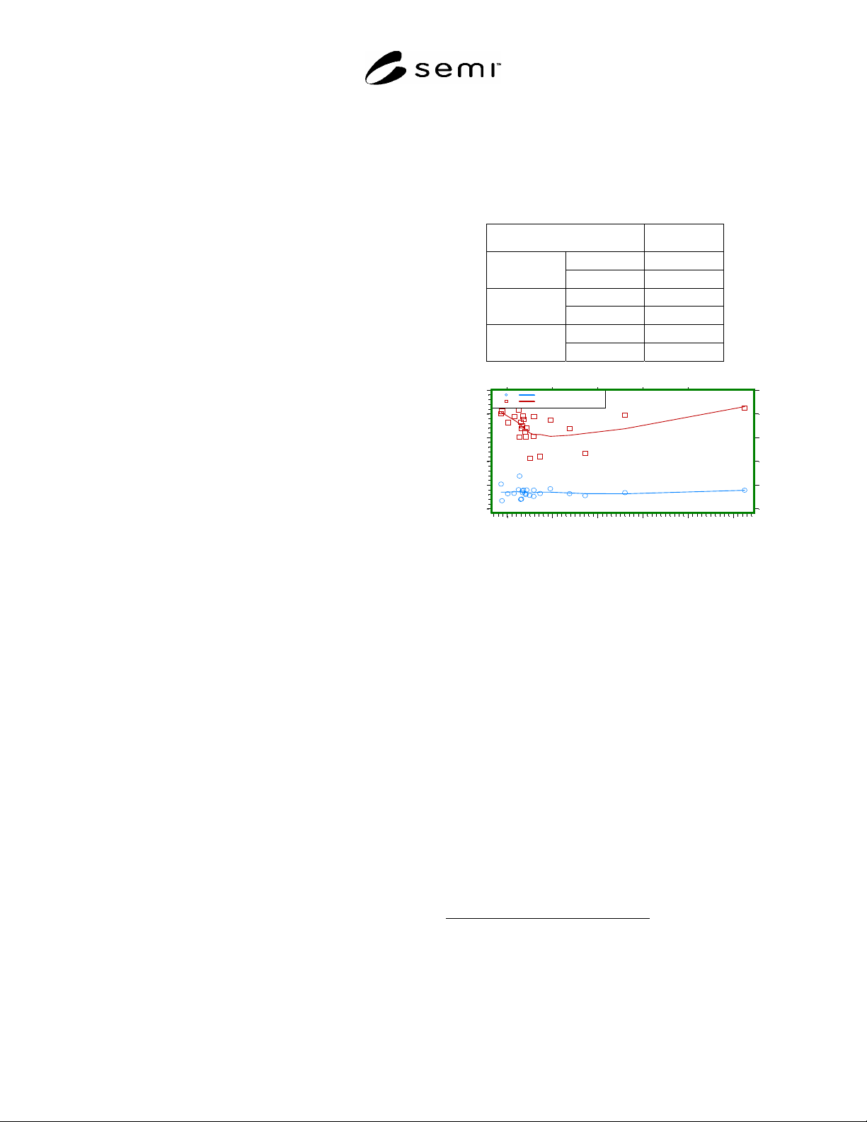
15.2 Eight laboratories measured warp. Warp value
ranges for these three subsets are shown in Table 1.
Each of the twenty-three wafers was measured three
times in succession (in three cassette-to-cassette
“passes”), on a single day on automatic measurement
systems in accordance with this test method.
15.3 All measurement data were acquired with 3 mm
nominal edge exclusion.
15.4 The number of laboratories, samples, and
determinations in this study met the minimum
requirements for determining precision prescribed in
ASTM Practice E 691.
15.5 The ranges of 95% confidence interval, within
which two measurements are considered statistically to
be the same, for within-laboratory repeatability (r) and
between-laboratory reproducibility (R) are shown in
Table 1.
15.6 Figure 2 contains plots of the 95% confidence
intervals for repeatability (r) and reproducibility (R)
against mean value of warp.
15.7 For more details, refer to the Research Report.
4
Table 1 Summary Warp Measurement Statistics
Parameter Warp
Smallest 4.30
Mean, m
Largest 31.25
Smallest 0.184
r, m
Largest 0.695
Smallest 1.112
R, m
Largest 2.097
Figure 2
Warp Repeatability & Reproducibility
16 Bias
16.1 Bias — No standards exist against which the bias
of this test method can be evaluated.
17 Keywords
non-contact measurement; semiconductor; shape;
silicon; wafers; warp
4 Available on request from SEMI Headquarters, Publications
Department, San Jose, CA, Fax: 408-943-7015. Request International
Standards Research Report F01-1016, ASTM Interlaboratory Round
Robin Experiment on Measuring Warp on Silicon Wafers by
Automated Noncontact Scanning and Measuring Flatness, Thickness
and Thickness Variation of Silicon Wafers by Automated Noncontact
Scanning.
Mean Warp,
m
r and R, m
D
V
N
O
C
A
W
R
T
J
L
H
F
K
Q
E
G
M
S
I
U
P
B
D
V
N
O
C
A
W
R
T
J
L
H
F
K
Q
E
G
M
S
I
U
P
B
5 1015202530
0.0
0.5
1.0
1.5
2.0
2.5
Repeatability
Reproducibility
SEMI MF1390-1104 © SEMI 2004 7
RELATED INFORMATION 1
MEASUREMENT ERRORS DUE TO DIFFERENCES IN DIAMETER AND
THICKNESS BETWEEN A REPRESENTATIVE WAFER AND A WAFER
UNDER TEST
NOTICE: This related information is not an official part of SEMI MF1390. This related information was approved
for publication by full letter ballot on April 22, 2004.
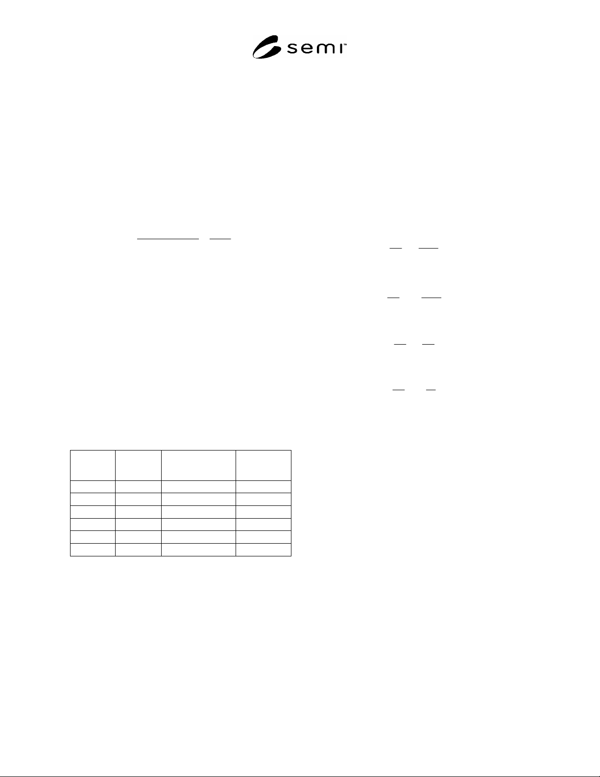
R1-1 The sag, or deflection induced by gravity at the
edge of a wafer supported at its center, in m, has been
estimated
3
as:
2
4
2
48
32
)103(
t
KD
Et
kgdD
S
(R1-1)
where:
S =
deflection , in m,
k = geometrical constant (=0.5854),
g = gravitational constant (980 cm/s
2
),
d = density of silicon (2.329 g/cm
3
),
E =
Young’s modulus (~1.610
12
dyne/cm
2
,
D = nominal wafer diameter, in mm, and
t =
nominal wafer thickness, in m.
K, the constant of proportionality is therefore equal to
7.83 10
3
m
3
/mm
4
. Table R1-1 gives estimated
values of sag in micrometers for 100 mm through 300
mm diameter wafers with thickness and diameter as
specified in SEMI M1.
Table R1-1. Estimated Sag, in
m, of Wafers of
Nominal Diameter and Thickness
Diameter,
mm
Thickness,
m
SEMI M1 Reference Estimated Sag,
m
300 775 SEMI M1.15 105.6
200 725 SEMI M1.9 23.8
150 675 SEMI M1.8 8.7
150 625 SEMI M1.13 10.1
125 625 SEMI M1.7 4.9
100 525 SEMI M1.5 2.8
R1-2 For small variations about the nominal values of
diameter and thickness, the relative change of the
gravity effect is 4 times the relative change of the
diameter and 2 times the relative change of thickness:
2
3
4
t
Kd
d
S
(R1-2)
and
3
4
2
t
Kd
t
S
(R1-3)
Therefore the relative changes are as follows:
d
d
S
S
4 (R1-4)
and
t
t
S
S
2 (R1-5)
R1-3 Table R1-2 gives examples of worst-case gravity
effect errors (in micrometers), for 100 mm through 300
mm diameter wafers with thickness and diameter toler-
ances as specified in SEMI M1.