semi合集-English.pdf - 第24页
SEMI E1.9-0701 E2 © SEMI 1994, 2004 4 r 5 ≤ 170 r 4 ≥ 170 boundary of right rear cassette side dom ain boundary of left rear cassette side do main front side of the cassette where wafers are accessed boundary of left fro…

SEMI E1.9-0701
E2
© SEMI 1994, 2004 3
5 Ordering Information
5.1 Intended Use — This standard is intended to
specify 300 mm cassettes over a reasonable lifetime of
use, not just those in new condition. For this reason, the
purchaser needs to specify a time period and the
number and type of uses to which the cassettes will be
put. It is under these conditions that the cassettes must
remain in compliance with the requirements listed in
Section 6.
5.2 Temperature Ranges — The purchaser of 300 mm
cassettes needs to specify two sets of temperatures to
which the cassettes might be exposed. An operating
temperature range is the set of environmental
temperatures in which the cassettes will remain in
compliance with the requirements listed in Section 6. A
temporary temperature range is the set of environmental
temperatures to which the cassettes can be exposed
such that when the cassettes return to the operating
temperature range, the cassettes will be in compliance
with the requirements listed in Section 6. Limits on
exposure times to elevated temperatures should be
specified. Also, the purchaser needs to specify a range
of temperatures for the wafers that might be inserted in
the cassettes.
5.3 Info Pad Configurations — The purchaser of 300
mm carriers needs to specify the desired info pad
configuration (up or down). See Appendix 1
(Application Notes).
6 Requirements
6.1 Kinematic Couplings — The physical alignment
interface on the bottom of the cassette consists of
features (not specified in this standard) that mate with
six pins underneath as defined in SEMI E57. Most of
the dimensions of the cassette are determined with
respect to the three orthogonal datum planes defined in
that standard: the horizontal datum plane, the facial
datum plane, and the bilateral datum plane. All of the
dimensions for the cassette are bilaterally symmetric
about the bilateral datum plane. The three features that
mate with the pins must provide a lead-in capability
that corrects a cassette misalignment no greater than
r19 in any horizontal direction. However, it is
recommended that robots placing cassettes on
kinematic couplings use as little of this lead-in
capability as possible to avoid wear.
6.2 Wafer Orientation and Numbering — The wafers
must be horizontal when the carrier is placed on the
coupling, and the wafers are numbered in increasing
order from bottom to top (so the bottom wafer is wafer
number 1, the next wafer up is wafer number 2, etc.).
After processing at a tool, each wafer should be
returned to the same slot from which it was taken.
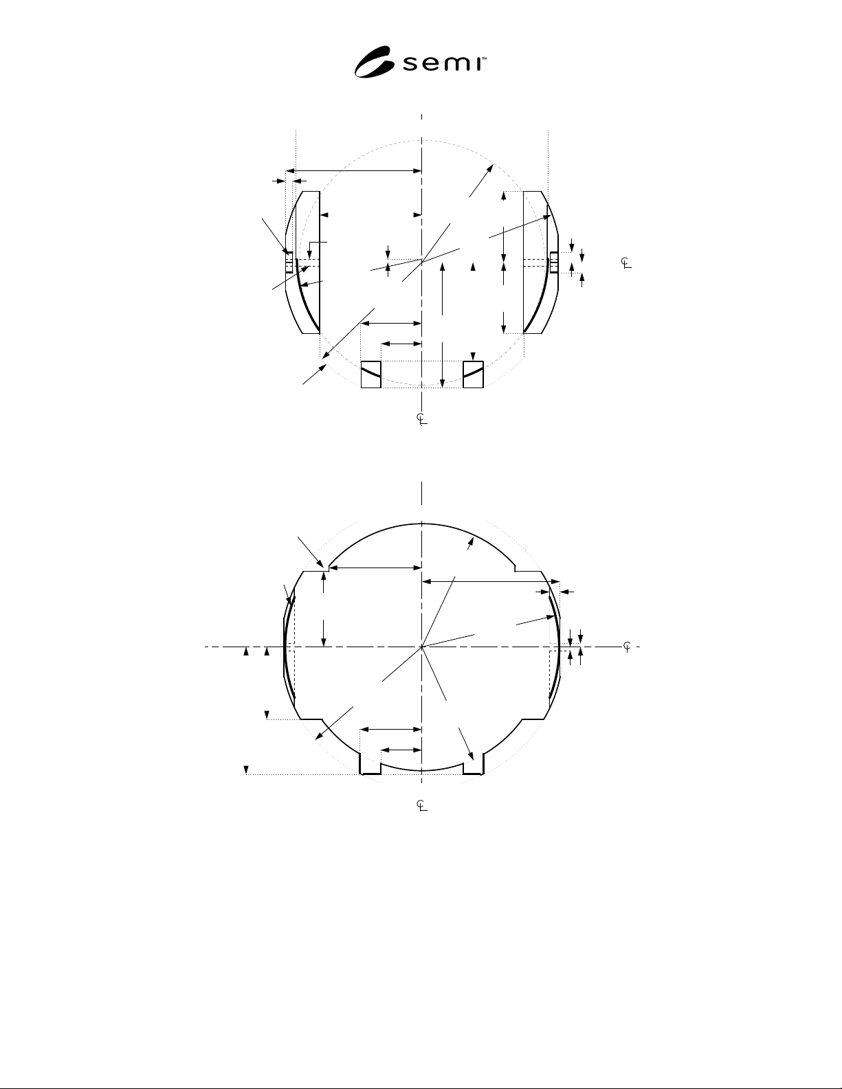
6.3 Cassette Sides — Figure 1 shows a cross-section of
the horizontal boundaries of the cassette side domains
(which contain the parts of the cassette higher than z6
above the horizontal datum plane and lower than z15
above the top wafer). In this and following figures, the
most heavy lines are used for surfaces that have
tolerances (not surfaces that have only maximum or
minimum dimensions). Table 1 defines the dimensions
shown in this and following figures. The maximum
protrusions of any part of the cassette from the nominal
wafer center line and from the bilateral datum plane is
r5 and x9, respectively. There are two optional side grip
pits on each side. For optically sensing whether a
cassette is properly in place, from left to right under the
bottom wafer is an optical cassette sensing hole. The
radius of this hole is given with both upper and lower
tolerances, but the upper tolerance is only to define a
minimum aperture that must be met at only one section
on each side. Other than through the optical cassette
sensing holes, the cassette bottom and side domains
must block any line of sight passing through both of the
two rectangles at x10 on each side bounded by z4, z20,
y2, and y3.
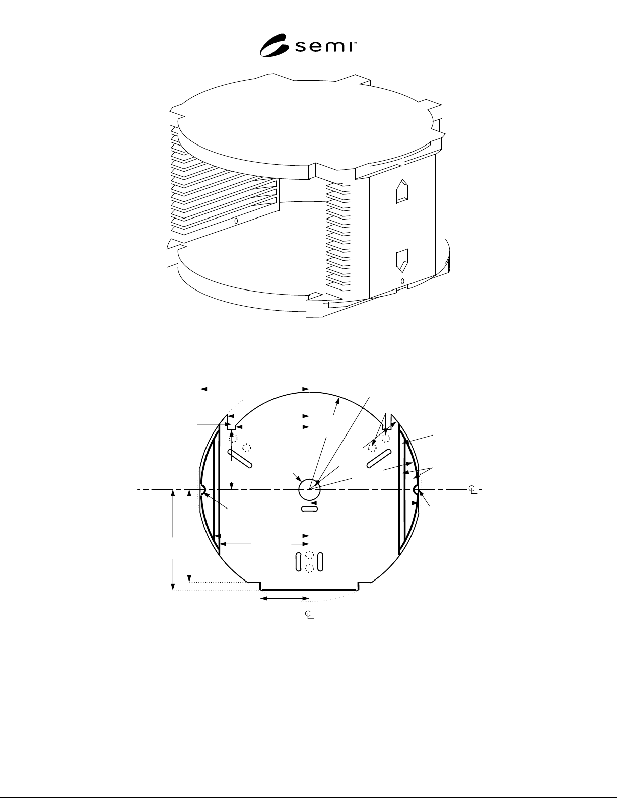
6.4 Cassette Top — Figure 2 shows a top view of the
horizontal boundaries of the cassette top domain which
contains any part of the cassette higher than z15 above
the top nominal wafer plane. The top robotic handling
flanges (optional), the side grip pits (optional), and
optical cassette sensing hole on the side can be seen in
Figure 3, which is an oblique view of the maximum
cassette dimensions (see Figure 14 to see how cassettes
need not take up all of that volume). The maximum
radial protrusions of the cassette top in the front and
rear are r6 and r12, respectively. Dimensions x6, x12
(shown in Figure 4), and y15 define a vertical path for
optically sensing wafers through the top and bottom
domains.
SEMI E1.9-0701
E2
© SEMI 1994, 2004 4
r5
≤170
r4
≥170
boundary of
right rear cassette
side domain
boundary of
left rear cassette
side domain
front side of the cassette where wafers are accessed
boundary
of left front
cassette
side domain
y6
≤152
wafer
pick-up area
y5
≥120
y4
≤85
x3 ≥125
x1
≥50
x2
≤75
boundary
of right front
cassette
side domain
reserved
for end-
effector
fingers
r1
≤151
facial
datum
plane
bilateral datum plane
r2 =152
r3 ≥r2 + 1
wafer set-down and
extraction
volumes
y1 ≤ 3
y2 =10±1
y3 =10±1
side grip pit
(optional, see
section 6.3)
x4 ≥8
r9
=2.5±.5
optical cassette
sensing hole
x9 ≤167
x10 =166 ±1
(at side grip pits)
y11
≤85
+1
–0
Figure 1
Cassette Side Domains
x6
≤112.5
y15
≤95
boundary
of cassette
top domain
y16
=155 ±1
r6
≤157
facial
datum
plane
front side of the cassette where wafers are accessed
y4
≤85
x1
≥50
x5
=76±1
bilateral datum plane
r5
≤170
optical wafer
sensing path
r11
=166 ±1
y8
=2±0.5
y7
=2±0.5
x9 ≤167
r12
≤152
x7 ≥12
robotic handling
flange (optional,
see section 6.4)
Figure 2
Cassette Top Domain
SEMI E1.9-0701
E2
© SEMI 1994, 2004 5
Figure 3
Oblique View of Maximum Cassette Dimensions
r8
=7.5±1
r7
≥
15
y16
=155 ±1
y23
≤
140
kinematic pins
r5
≤
170
boundary
of cassette
bottom domain
front side of the cassette where wafers are accessed
conveyor
surface
facial
datum
plane
r6
≤
157
bilateral datum plane
x
5
=76 ±1
x
16 =140±1
pod latch-pin hole
x
15
≤
132
fork-lift
pick-up
area
r10
=166±1
fork-lift
pin hole
x
9
≤
167
x
6
≤
112.5
y15
≤
95
optical wafer
sensing path
x
12
≥
125
x
11 = 166
Figure 4
Cassette Bottom Domain