semi合集-English.pdf - 第5403页
SEMI M57-0705 © SEMI 2004, 2005 7 5.2 Purchase orders furnished to t his guide shall also include the it e ms shown i n Table 1 for the fi nished anneale d wafers, and other items as agreed between supplier and customer.…
SEMI M57-0705 © SEMI 2004, 2005 6
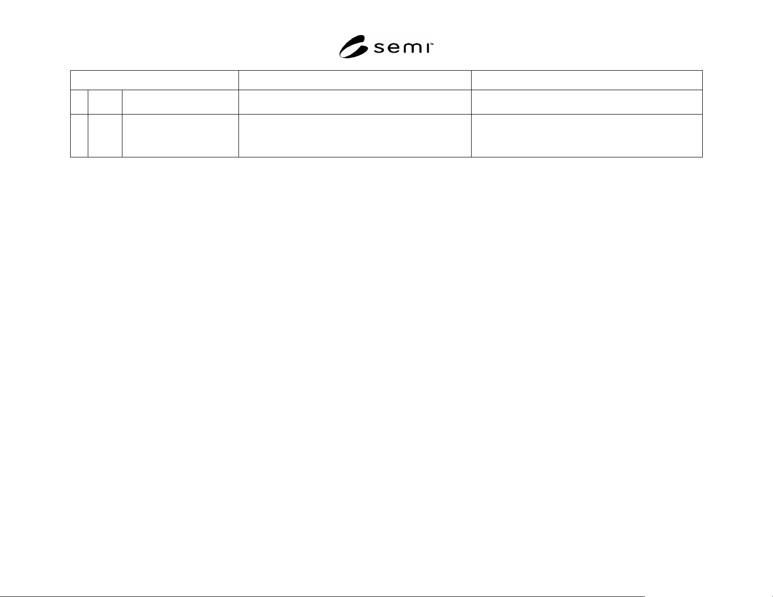
ITEM SPECIFICATION MEASUREMENT METHOD
5-7.3 BMD Density
Range [ ] 10
[ ]
to [ ] 10
[ ]
Unit
Unit: [ ]cm
2
; [ ]cm
3
Test Cycle: SEMI MF1239 [ ]A, [ ]B;
Other: (specify)________
5-7.4 Other Post-Anneal
Characteristics
Surface boron depletion, dissolved hydrogen in the case of
hydrogen annealed wafer, post-annealed oxygen, and silicon
nitride precipitates and defects in the case of nitrogen-doped
silicon may be discussed between supplier and customer.
As discussed between supplier and customer.
#1
If specified as polished, this term is meant to imply a surface condition and not a particular processing technique. If desired, a quantitative measure of surface finish may optionally be indicated by
specifying the rms microroughness over a specified spatial frequency (or wavelength) range. Because a standardized test method has not yet been developed for this metric, both values and test
procedures, including sampling plan and detrending procedures, shall be agreed upon between supplier and customer.
#2
Flatness Acronyms are defined in the Flatness Decision Tree in Appendix 1 of SEMI M1.
#3
In today’s technology, it may be possible to inspect for some of these items using automated surface scanning inspection systems (SSIS). Such systems should be calibrated according to SEMI M53
using polystyrene latex spheres deposited in accordance with SEMI M58. Some indication of the defects separable by such instruments is provided in SEMI M35; however, a standard test procedure has
yet to be developed. Application of automated inspection with the use of an SSIS must be agreed upon between supplier and customer.
SEMI M57-0705 © SEMI 2004, 2005 7
5.2 Purchase orders furnished to this guide shall also include the items shown in Table 1 for the finished annealed
wafers, and other items as agreed between supplier and customer.
5.3 In addition, the purchase order must indicate the test method to be used in evaluating each of those items for
which alternate test procedures exist.
5.4 The following items must also be included in the purchase order:
5.4.1 Lot acceptance procedures.
5.4.2 Certification (if required).
5.4.3 Packing and shipping container labeling requirements.
6 Requirements Specifying Silicon Annealed Wafers
6.1 Table 2 provides a guide for specifying polished silicon annealed wafers for the 180 nm, 130 nm, and 90 nm
technology generations. A parameter not listed in this table need not be specified.
6.2 It is also essential to specify appropriate test methods in each case. Defaults for test method selection are given
in §8.
6.2.1 The line items with numbers beginning with “2-” are listed in Part 2 of the Silicon Wafer Specification Format
for Order Entry, SEMI M1, Table 1. The line items with numbers beginning with “5-” are listed in Part 5 of this
format, included herein as Table 1.
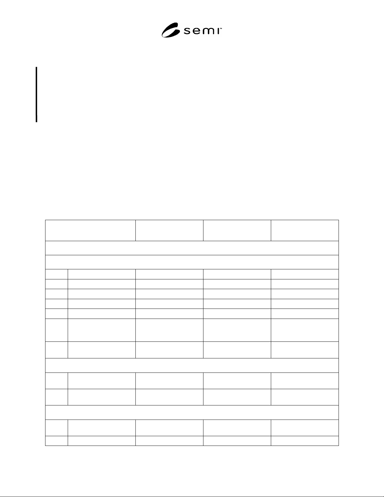
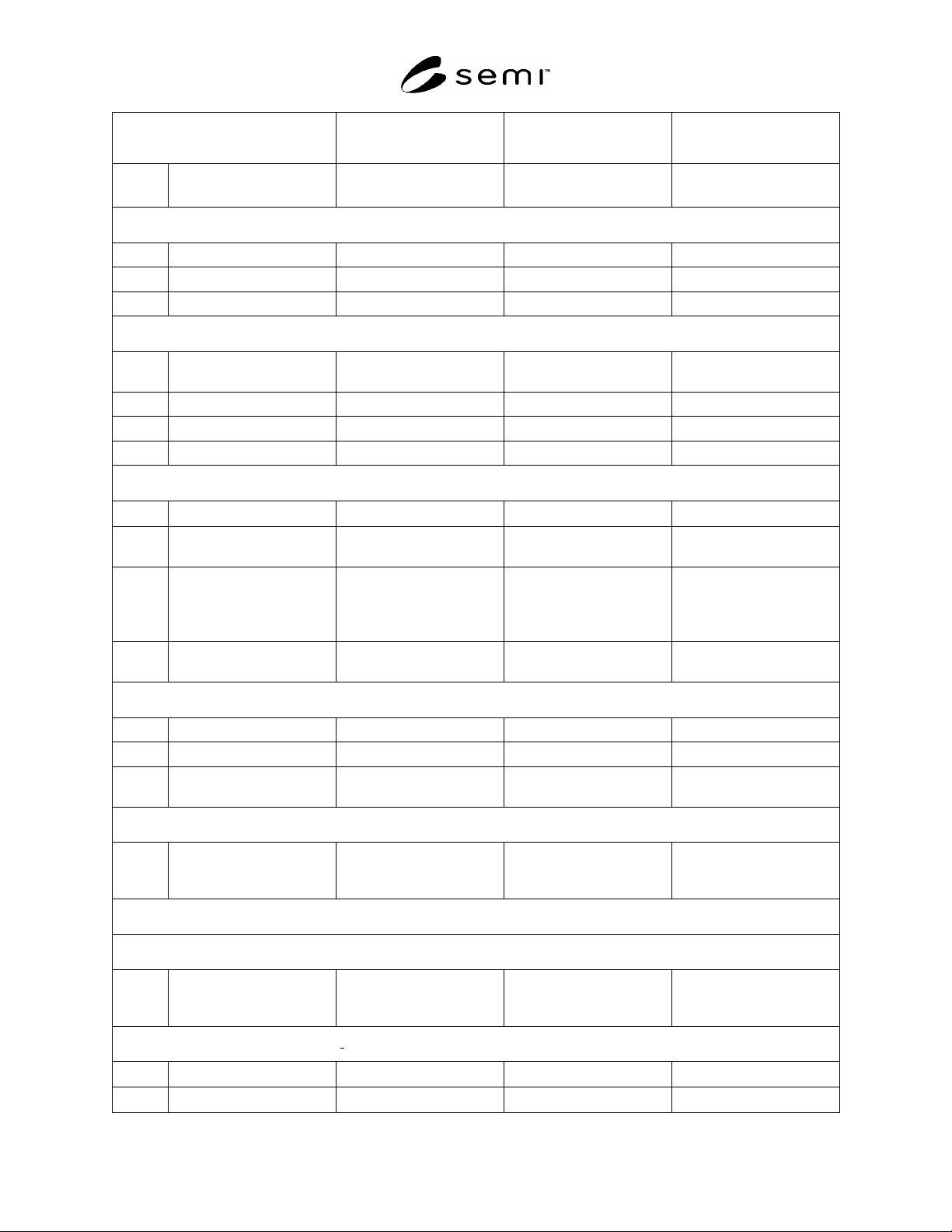
Table 2 Guide for Specifying Polished Silicon Annealed Wafers for the 180 nm, 130 nm and 90 nm
Technology Generations
Item 180 nm Technology
Generation
130 nm Technology
Generation
90 nm Technology
Generation
PRE-ANNEAL STATE (POLISHED WAFER)
2-1 GENERAL CHARACTERISTICS
2-1.1 Growth Method Cz or MCz Cz or MCz Cz or MCz
2-1.3 Crystal Orientation (100) (100) (100)
2-1.4 Conductivity Type p-type p-type p-type
2-1.5 Dopant Boron Boron Boron
2-1.6 Nominal Edge Exclusion 3 mm 3 mm 2 mm
2-1.7 Co-dopant in Crystal None, Nitrogen and/or
Carbon (as agreed between
supplier & customer).
None, Nitrogen and/or
Carbon (as agreed between
supplier & customer).
None, Nitrogen and/or
Carbon (as agreed between
supplier & customer).
2-1.8 Wafer Surface Orientation On-orientation:
0.00 1.00
On-orientation:
0.00 1.00
On-orientation:
0.00 1.00
2-2 ELECTRICAL CHARACTERISTICS
2-2.1 Resistivity (Center point) As agreed between supplier
& customer.
As agreed between supplier
& customer.
As agreed between supplier
& customer.
2-2.2 Radial Resistivity
Variation
#1
20% 20% 20%
2-3 CHEMICAL CHARACTERISTICS
2-3.1 Oxygen Concentration/
Calibration Factor
As agreed between supplier
& customer.
As agreed between supplier
& customer.
As agreed between supplier
& customer.
2-3.2 Radial Oxygen Variation
#2
±10%, 10 mm from the edge ±10%, 10 mm from the edge ±10%, 10 mm from the edge
SEMI M57-0705 © SEMI 2004, 2005 8
Item 180 nm Technology
Generation
130 nm Technology
Generation
90 nm Technology
Generation
2-3.3 Carbon Concentration
(Background
#3
)
0.5 ppma 0.5 ppma 0.5 ppma
2-4 STRUCTURAL CHARACTERISTICS
2-4.3 Lineage None None None
2-4.4 Twin Boundary None None None
2-4.5 Swirl None None None
2-5 WAFER PREPARATION CHARACTERISTICS
2-5.1 Wafer ID Marking As agreed between supplier
and customer.
SEMI T7 plus optional
alphanumeric mark.
SEMI T7 plus optional
alphanumeric mark.
2-5.2 Front Surface Thin Films None None None
2-5.4 Extrinsic Gettering None None None
2-5.5 Backseal None None None
2-6 DIMENSIONAL CHARACTERISTICS
2-6.1 Diameter
200.00 mm 0.20 mm 300.00 mm 0.20 mm
#4
300.00 mm 0.20 mm
#4
2-6.6 Edge Profile As agreed between supplier
& customer.
As agreed between supplier
& customer.
As agreed between supplier
& customer.
2-6.7 Thickness
725 m 20 m
(Notched type wafers) or
675 m 15 m
(Flatted type wafers)
775 m 20 m 775 m 20 m
2-6.8 Total Thickness Variation
(TTV)
10 m, max 10 m, max 10 m, max
2-9 BACK SURFACE INSPECTION CHARACTERISTICS
2-9.1 Edge Chips None None None
2-9.8 Brightness (Gloss) Not specified 0.80
#5
0.80
#5
2-9.9 Scratches (macro) —
cumulative length
0.25 diameter 0.25 diameter 0.25 diameter
5-1 ANNEALING CONDITIONS
5-1.1 Annealing Atmosphere Hydrogen, Argon, or Other
(as agreed between supplier
& customer).
Hydrogen, Argon, or Other
(as agreed between supplier
& customer).
Hydrogen, Argon, or Other
(as agreed between supplier
& customer).
POST-ANNEAL STATE
5-2 POST-ANNEAL WAFER PREPARATION CHARACTERISTIC
5-2.1 Edge Surface Condition Acid Etched or Polished
#6
(as agreed between supplier
& customer).
Acid Etched or Polished
#6
(as agreed between supplier
& customer).
Acid Etched or Polished
#6
(as agreed between supplier
& customer).
5-3 POST ANNEAL DIMENSIONAL CHARACTERISTICS
5-3.1 Warp
75 m 100 m
#7
100 m
#7
5-3.2 Site Flatness
#8
SFQR 180 nm SFQR 130 nm SFQR 90 nm