semi合集-English.pdf - 第4845页
SEMI M1-0305 © SEMI 1978, 2005 21 6.5.1.4. 2 Single d ensity dot matrix, 5 dots horizontal and 9 dots vertical, shall be used. 6.5.1.4. 3 Dot diameter shall be the sam e as that used for the t w o-dimensi onal mat r ix c…
SEMI M1-0305 © SEMI 1978, 2005 20
6.1.7.4.2 Uniform, maximum channeling along the [100] axis perpendicular to the (100) wafer surface is strongly
dependent on strict adherence to a 0 tilt angle. To achieve maximum channeling, crystallography requires the
orientation to be within ±0.1 of a <100> direction. Also, the customer must remove all overlying oxide, nitride,
poly, etc., layers from the wafer prior to a channeling implant. The customer must maintain very rigid control of the
ion implant equipment angle setting in order to achieve maximum channeling across the wafer.
6.1.7.5 The tolerance of ±0.1 is derived from experimental ion implant profile data and ion implant modeling
activity for implants into (100) silicon wafers. The ranges for which data was obtained are given in Table 2.
6.2 Electrical Characteristics
6.2.1 The center-point room temperature resistivity of the
wafers shall conform to the nominal and tolerance values
specified on the purchase order.
6.2.2 The wafers shall conform to any requirements
specified on the purchase order for radial resistivity
variation, resistivity striations and minority carrier
lifetime.
6.3 Chemical Characteristics
6.3.1 The wafers shall conform to any requirements specified on the purchase order for oxygen concentration, radial
oxygen variation, carbon concentration, and, for heavily doped (low resistivity) n-type silicon wafers only,
compensating boron concentration.
6.4 Structural Characteristics
6.4.1 The wafers shall conform to any requirements specified on the purchase order for dislocation etch pit density,
slip, lineage, twin, swirl, shallow pits, oxidation induced stacking faults (OSF), oxide precipitates or bulk
microdefects (BMD), interstitial oxygen reduction upon appropriate heat treatment, and bulk defects by X-ray
topoography.
6.5 Wafer Preparation Characteristics
6.5.1 Wafer ID Marking—Where wafer ID marking is specified on the purchase order, the kind of marking must be
indicated.
6.5.1.1 Where alphanumeric marking is specified for wafers of 200 mm diameter and smaller, the code character
properties and code field location shall conform either to SEMI M13 or to SEMI M12, as specified on the purchase
order.
6.5.1.2 Where back-surface bar code marking is specified for wafers of 200 mm diameter and smaller, the code
symbol and its location shall conform to SEMI T1.
6.5.1.3 Where two-dimensional matrix code marking is specified for wafers of 200 mm diameter and smaller, the
code symbol and its location shall conform to SEMI T2.
6.5.1.4 All 300 mm diameter wafers (wafer category 1.15, see Table 9) shall be marked with a two-dimensional
matrix code symbol on the back surface outside the fixed quality area as soon after slicing as practical in the manner
specified in SEMI T7 in order to provide both identification of these wafers and traceability of each wafer back to
the ingot from which it was cut. The back surface is identified as the wafer surface with the two-dimensional matrix
code symbol.
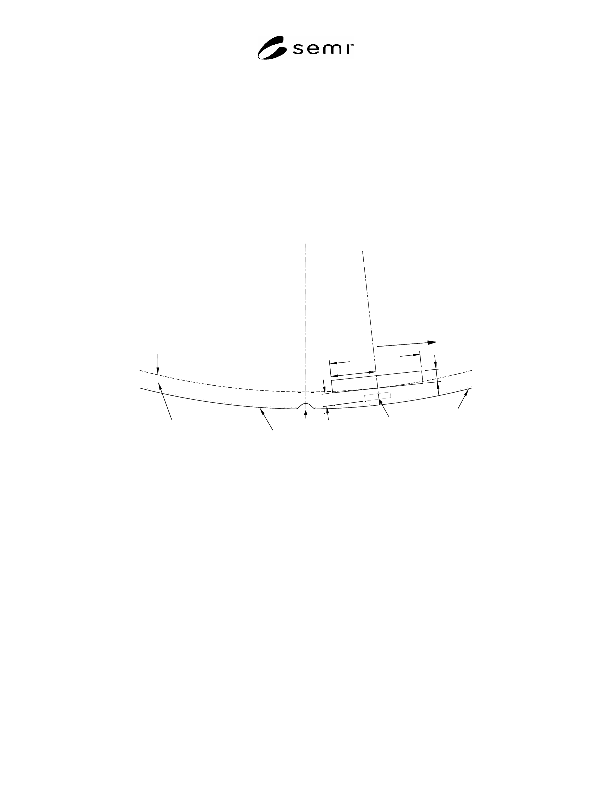
6.5.1.4.1 Optionally, the user may specify an additional back-surface mark
as shown in Figure 3. This mark
contains alphanumeric characters with:
The same message characters as the SEMI T7 mark and appropriate checksum characters as defined by SEMI
M12 and
Character string as specified in SEMI M12.
NOTE 1: It is expected that this optional alphanumeric mark will not be used after users have developed successful experience
with SEMI T7 mark usage.
Table 2 Energy Ranges for Ion Implant Modeling
Species Energy Range (keV)
B 15–80
BF
2
15–65
As 15–180
SEMI M1-0305 © SEMI 1978, 2005 21
6.5.1.4.2 Single density dot matrix, 5 dots horizontal and 9 dots vertical, shall be used.
6.5.1.4.3 Dot diameter shall be the same as that used for the two-dimensional matrix code symbol (see 6.5.1.4).
6.5.1.4.4 Character dimensions shall be as defined in Table 1 of SEMI M12 (nominal spacing = 1.42 mm, nominal
width = 0.812 mm, nominal height = 1.624 mm).
6.5.1.4.5 Mark location (center of bottommost dot rows) relative to the reference point of the SEMI T7 mark shall
be 1.40 0.05 mm toward the wafer center, as shown in Figure 3.
6.5.1.4.6 Mark field height, as defined by the distance between the centers of the topmost and bottommost dot rows
of the A/N characters, shall be 1.62 0.03 mm (Note 2).
6.5.1.4.7 Mark field length, as defined by the distance between the centers of the leftmost and rightmost dot
columns of the A/N characters, shall be 16.43 0.07 mm.
0
mm
0
5
A
/
N
r
e
a
d
d
i
r
e
c
t
i
o
n
1
6
.
4
3
±
0
.
0
7
5.0° ± 0.1° from
Orientation Fiducial Axis
1
4
8
.
9
5
±
0
.
1
5
f
r
o
m
d
a
t
a
m
a
t
r
i
x
c
o
d
e
s
y
m
b
o
l
r
e
f
e
r
e
n
c
e
p
o
i
n
t
t
o
w
a
f
e
r
c
e
n
t
e
r
All dimensions
in millimeters
unless other-
wise indicated
O
u
t
e
r
P
e
r
i
p
h
e
r
y
o
f
F
Q
A
Edge Exclusion Area
5 mm
Edge Profile Region
Notch
A
/
N
M
AR
K
Orientation Fiducial Axis
[011] ± 1.0°
Wafer Periphery
1
.
6
2
±
0
.
0
3
Wafer Back Surface
8
.
2
2
±
0
.
0
5
Referenc e
Point of SEMI T7 Mark
T
7
M
A
R
K
1
.
4
0
±
0
.
0
5
NOTE: A/N mark field dimensions are defined by the centers of the topmost and bottommost dot rows and
the center of the leftmost and rightmost dot columns of the A/N characters. The field dimensions are more
tightly controlled than those of a field constructed using SEMI M12. This results from the availability of
laser marking capabilities not available when SEMI M12 was developed. In addition, the tolerance on the
field dimensions is not cumulative.
Figure 3
Optional A/N Code Field Location on Back Surface of Notched 300 mm Diameter Wafer (Category 1.15)
NOTE 2: The overall length tolerance of the A/N mark is more stringent than that in SEMI M12. Also the height tolerance of the
overall mark imposes tighter skew and offset tolerances than are required in SEMI M12.
6.5.1.4.8 The mark-field shall be centered on the radius that passes through the reference point of the SEMI T7
mark as shown in Figure 3.
6.5.1.4.9 Character baseline shall be toward wafer OD and parallel with the row of the SEMI T7 mark that contains
that mark’s reference point.
6.5.2 Other — The wafers shall conform to any requirements specified on the purchase order for any other wafer
preparation characteristics including front surface thin films, denuded zone, extrinsic gettering, backseal, annealing,
and edge and back surface conditions.
SEMI M1-0305 © SEMI 1978, 2005 22
6.6 Dimensional Characteristics
6.6.1 Dimensions and Fiducials — The wafers shall conform to the dimensions, dimensional tolerances, and
fiducial (flat or notch) characteristics and locations as specified in the purchase order.
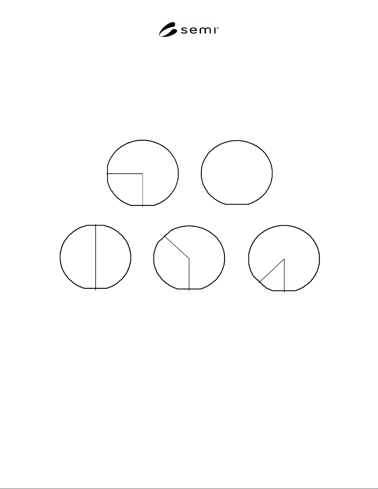
6.6.1.1 Where secondary flats are specified, they shall be located as shown in Figure 4.
6.6.1.2 Where notches are specified, they shall conform to the dimensions in Figure 5.
6.6.2 Edge Profile — The edge profile of edge-profiled wafers shall conform to the following requirements at all
points on the wafer periphery (except interior portions of notches, if present).
6.6.2.1 The SEMI Wafer Edge Profile Template is shown in Figure 6. There are two sets of dimensions for the
template: T/3 and T/4, where T is the nominal thickness of the wafer (see Tables 4 through 9 for values of the
nominal thickness for various wafer categories).
90
CW
180 CW
135 CW
45 CW
a. (
100) p-type b. (111) p-type
c. (100) n-type d. (100) n-type e. (111) n-type
(wafers 125 mm diameter or less) (150 mm diameter wafers only)
NOTE 1: Secondary flat location for 150 mm diameter (100) n-type wafers changed from configuration c to configuration d
effective January 1, 1990.
NOTE 2: The angular position of the center point of the secondary flat is given in Tables 4 through 6 both in terms of the
clockwise angle from the primary flat, located at the bottom of each figure, to the secondary flat and the angle,
, from the
positive x-axis of the wafer coordinate system as defined by SEMI M20 (at 3 o’clock) to the secondary flat.
Figure 4
Secondary Flat Locations