semi合集-English.pdf - 第6099页
SEMI G19-0997 © SE MI 1980, 1997 4 tolerances for unt aped frames and Table 2 tolerances for taped f ra mes . Table 1 Toler ances for Untaped Fr ames No. of Leads Strip Wi dth Lead Tip Cop lanarity 8 - 16 600"–1.00 …
SEMI G19-0997 © SEMI 1980, 19973
5 Dimensions
See applicable leadframe drawing as referred to in the
ordering information.
6 Defect Limits and Parame ters (see SEMI
G10 to Measure)
6.1 Minimum Flat Wire Bonding Area — 0.203 mm
(0.008") or 80% of nominal lead width, whichever is
greater in width and 0.635 mm (0.025") in length.
Undercut is an unavoidable process of etching. The
above parameters are applicable only so long as the flat
surface area is obtainable using the formula of Figure 4.
The “radiusing” effect of the etching process will round
off the tips and, therefore, the length of the flat area
should be measured by starting back from the tip 0.254
mm (0.010").
NOTE: 0.008" flat is desirable. In order to achieve 0.008" flat,
on 0.010" thick material, it is necessary to have a design
width of 0.022" center to center, giving a 0.012" wide lead
and 0.010" wide space.
6.2 Horizontal Lead Spacing and Location
6.2.1 Spacing between leads to be 0.152 mm (0.006")
minimum after plating.
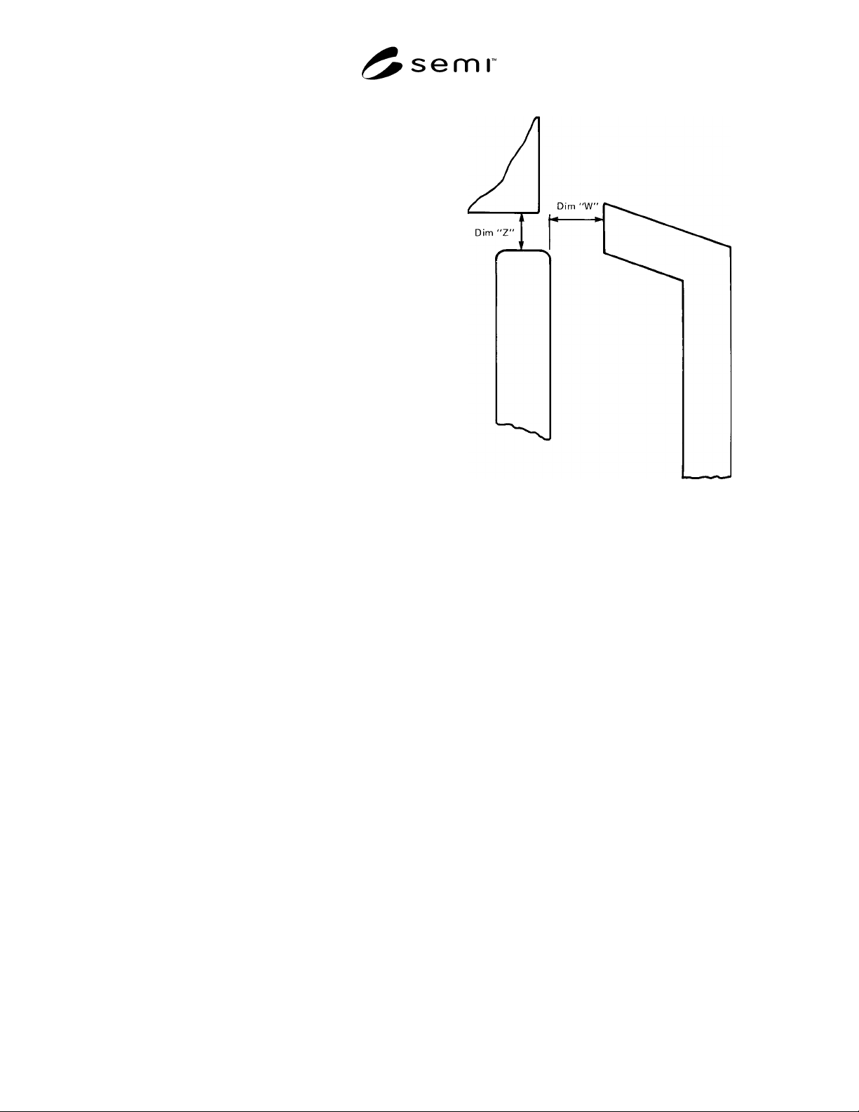
6.2.2 Metal to metal clearance (Dimension “W”
Figure 7) minimum clearance shall be the greater of
0.152 mm (0.006") or the drawing dimension “W”
minus 0.102 mm (0.004"). In determining dimension
“W,” the tolerance limits (max. vs. min.) shown on the
drawing shall be used in the calculation.
Figure 7
Metal to Metal Clearance
6.3 Lead Twist — Not to exceed 2° 30' or 0.0004"
(0.010 mm) per 0.010" (0.254 mm) of lead width.
6.4 Die Attach Pad Tilt & Flatness
6.4.1 Tilt — 0.001" (0.025 mm) maximum per 0.100"
(2.54 mm) of length or width in the undepressed state
and 0.002" (0.050 mm) max per 0.100" (2.54 mm) of
length or width in the depressed state when measuring
from corner to corner. The corners are defined as
0.005" (0.127 mm) from each edge.
6.4.2 Flatness — 0.0004" (0.010 mm) maximum
difference per 0.100" (2.54 mm) of length or width
when measuring from center to average of four corners.
The corners are defined as 0.005" (0.127 mm) from
each edge.
6.5 Die Attach Pad Offset or Depression — (if
applicable) — ± 0.002" (0.050 mm) as measured from
the center of the pad to a point on the bar pad support
strip. The nominal recommended offset is 0.015" (0.381
mm).
6.6 Lead and Die Attach Pad Coplanarity — See
SEMI G10 for measurement procedure.
6.6.1 Lead Planarity — The lead tips as measured in
the center of the flat wirebonding area must be within
the following tolerances of the “Z” plane. Use Table 1
SEMI G19-0997 © SEMI 1980, 1997 4
tolerances for untaped frames and Table 2 tolerances
for taped frames.
Table 1 Tolerances for Untaped Frames
No. of
Leads Strip Width Lead Tip Coplanarity
8 - 16 600"–1.000"
(15.24 mm–25.4 mm)
+ 0.004"/-0.004"
(0.101 mm)
18 - 22 1.070"– 1.020"
(27.18 mm–25.91 mm)
+ 0.005"/-0.005"
(0.127 mm)
22 1.270"–1.300"
(32.26 mm– 33.02 mm)
+ 0.0065"/-0.0065"
(0.165 mm)
24 1.470"–1.500"
(37.34 mm–38.10 mm
+ 0.0075"/-0.0075"
(0.191 mm)
28 1.670"–1.700"
(42.42 m–43.18 mm)
+ 0.0085"/-0.0085"
(0.216 mm)
40 & up 2.270"–2.300"
(57.66 mm–58.42 mm)
+ 0.015"/-0.007"
(+0.381 mm/-0.178 mm)
Table 2 Tolerances for Taped Frames
No. of
Leads Strip Width Lead Tip Coplanarity
28 1.670"–1.700"
(42.42 mm–43.18 mm)
+0.007"/-0.005"
(+187 mm/-0.127 mm)
40 & up 2.270"–2.300"
(57.66 mm–58.42 mm)
+0.010"/0.005"
(+0.254 mm/-0.127
mm)
NOTE: It is recommended that 40 leads and more be taped
prior to bonding.
6.6.2 Die Attach Pad Planarity
6.6.2.1 The die attach pad when measured at the center
must be within the tolerances of the “Z” plane as shown
in Table 3.
Table 3 Pad Planarity Tolerances
No. of Leads Pad Planarity
8 - 16 +0.003"/-0.005"
(+0.076 mm/-0.127 mm)
18 - 20 +0.006"/-0.003"
(+0.152 mm/-0.076 mm)
22 - 40 +0.006"/-0.003"
(+0.152 mm/-0.076 mm)
48 +0.006"/-0.003"
(+0.152 mm/-0.076 mm)
64 +0.006"/-0.003"
(+0.152 mm/-0.076 mm)
6.6.2.2 Die attach pads utilizing the four point tie
design (support bars to both dambars) shall meet ±
0.002" (0.051 mm) of the “Z” plane.
6.7 Material — Thickness shall be as shown in Table
4.
Table 4 Material Thickness
Parameters 0.010"
(0.254 mm)
0.015"
(0.381 mm)
0.020"
(0.508 mm)
Thickness ± 0.0003"
(0.0076 mm)
± 0.0004"
(0.0102 mm)
± 0.0005"
(0.0127 mm)
Strip Width
2.0" (50.8 mm) ± 0.002"
(0.051 mm)
± 0.002"
(0.051 mm)
± 0.002"
(0.051 mm)
2.0" (50.8 mm) ± 0.003"
(0.076 mm)
± 0.003"
(0.076 mm)
± 0.003"
(0.076 mm)
6.8 Crossbow — Shall not exceed the dimensions
given in Table 5. If a certain width is not shown, 1% of
the leadframe width shall apply.
Table 5 Maximum Crossbow Dimensions
No. of
Leads Strip Width Max. Crossbow
8 0.600" (15.24 mm) 0.005" (0.127 mm)
14 - 16 0.970"/1.00" (24.64
mm/25.40 mm)
0.005" (0.127 mm)
18 1.070"/1.100" (27.18
mm/27.94 mm)
0.005" (0.127 mm)
20 1.170"/1.200"(29.72
mm/30.48 mm)
0.010" (0.254 mm)
22 1.270"/1.300"(32.26
mm/33.02 mm)
0.010" (0.254 mm)
24 1.470"/1.500"(37.34
mm/38.10 mm)
0.010" (0.254 mm)
28 1.670"/1.700"(42.42
mm/43.18 mm)
0.010" (0.254 mm)
40 2.270"/2.300"(56.66
mm/58.42 mm)
0.010" (0.254 mm)
48+ 2.400"/2.670"(60.96
mm/67.82 mm)
0.010" (0.254 mm)
6.9 Progression — Progression over the (# of) steps in
the strip should be within ± 0.051 mm (0.002") and
non-cumulative.
6.10 Pits (Indentations) — Pits and imperfections
cannot affect leadframe strength regardless of size (see
Figure 6).
6.10.1 Critical Bond Area — 0.635 mm (0.025") of
the finger tips + 0.508 mm (0.020") border of die attach
pad; nothing greater than 0.0005" (0.0127 mm)
diameter × 0.0076 mm (0.0003") in depth; not more
than 1 pit.

SEMI G19-0997 © SEMI 1980, 19975
Application Note: There is a question regarding the ability of
material suppliers to meet this specification. Revision of this
specification is under review.
6.10.2 Die Attach Pad — Functional side inside 0.508
mm (0.020") border; nothing greater than 0.127 mm
(0.005") diameter × 50% metal thickness in depth; not
more than 2 pits.
6.10.3 Die Attach Pad — Nonfunctional side; nothing
greater than .508 mm (0.020") × 50% of metal
thickness in depth; not more than 3 pits; cannot affect
leadframe strength regardless of size (i.e., pit cannot be
located within 0.127 mm (0.50") of pad support bar
attachments).
6.10.4 Internal leadframe areas where design width is
0.635 mm (0.025") or more, must be less than 0.381
mm (0.015") × 50% metal thickness in depth; if design
width is less than 0.635 mm (0.025"), area must be 50%
of design width. Cannot affect leadframe strength
regardless of size.
6.10.5 Major Lead Areas (outside dambar) —
Nothing greater than 0.127 mm (0.005") × 50% of
metal thickness in depth; nothing greater than 0.254
mm (0.010") on shoulder above taper. Cannot affect
leadframe strength regardless of size.
6.10.6 Dambar — Pit cannot extend all the way across
the bar.
6.11 Mold Locating Holes — Conventional mold
damage design dictates that gating is opposite pin #1;
therefore, the mold locating holes must be in the rail
adjacent to pin #1. In order to minimize gate flashing
between the mold and the rail edge, a specific tolerance
of ± 0.051 mm (0.002") is required from the centerline
of the mold hole to the opposite rail edge.
6.12 Strip Length — Strip length cut off shall be
within 0.005", lead tip to lead tip centerline (excluding
rails). The rail cut off length shall be within + 0.635
mm (0.025") unless otherwise specified by the user.
7 Sampling
Sampling will be determined between supplier and
purchaser.
8 Packaging and Marking
8.1 Packaging — Leadframes must be packaged in
containers designed and constructed to prevent damage
and/or contamination. Specific protection must be
provided against crushing, exposure to moisture, and
mixture gases.
8.2 Marking — The outer containers shall be clearly
marked to identify the user stock number, user purchase
order number, drawing number, supplier lot number,
and reel numbers within the carton. Additional
information required should be specified by the user.
NOTICE: These standards do not purport to address
safety issues, if any, associated with their use. It is the
responsibility of the user of these standards to establish
appropriate safety and health practices and determine
the applicability of regulatory limitations prior to use.
SEMI makes no warranties or representations as to the
suitability of the standards set forth herein for any
particular application. The determination of the
suitability of the standard is solely the responsibility of
the user. Users are cautioned to refer to manufacturer’s
instructions, product labels, product data sheets, and
other relevant literature respecting any materials
mentioned herein. These standards are subject to
change without notice.
The user’s attention is called to the possibility that
compliance with this standard may require use of
copyrighted material or of an invention covered by
patent rights. By publication of this standard, SEMI
takes no position respecting the validity of any patent
rights or copyrights asserted in connection with any
item mentioned in this standard. Users of this standard
are expressly advised that determination of any such
patent rights or copyrights, and the risk of infringement
of such rights, are entirely their own responsibility.
Copyright by SEMI® (Semiconductor Equipment and Materials
International), 3081 Zanker Road, San Jose, CA 95134. Reproduction o
f
the contents in whole or in part is forbidden without express written
consent of SEMI.