semi合集-English.pdf - 第7266页
SEMI MF671-0705 © SEMI 2003, 2005 3 7.1.4 An overlay, with refere nce lines perpendicular to each other intersecting at th e center, and ten calibrated divisions on the vert ical reference line above and below center, co…

SEMI MF671-0705 © SEMI 2003, 2005 2
4 Referenced Standards and Documents
4.1 SEMI Standards
SEMI M1 — Specifications for Polished Monocrystalline Silicon Wafers
SEMI M59 — Terminology for Silicon Technology
4.2 ANSI Standard
ANSI/ASQC Z1.4 — Sampling Procedures and Tables for Inspection by Attributes
1
4.3 ASTM Standard
E 122 — Practice for Choice of Sample Size to Estimate a Measure of Quality for a Lot or Process
2
4.4 DIN Standard
DIN 50441, Part 4, — Measurement or the Geometric Dimensions of Semiconductor Wafers: Diameter and Flat
Depth of Wafers
3
NOTICE: Unless otherwise indicated, all documents cited shall be the latest published versions.
5 Terminology
5.1 Definitions
5.1.1 offset (of the end region of a flat on a silicon wafer) — a perpendicular deviation at either end region of a flat
from the horizontal reference line, used to define the flat boundaries.
5.1.2 Other terms relating to silicon technology are defined in SEMI M59.
6 Summary of Test Method
6.1 The specimen is aligned on an optical comparator. One end of the projected image of the flat is positioned on a
reference point on the viewing screen. The micrometer reading is recorded, and the stage is manipulated to scan to
the opposite end of the flat where the micrometer reading is again recorded. Flat length is the difference between
the first and second readings.
7 Apparatus
7.1 Shadowgraph Comparator — Equipped as follows:
7.1.1 20× Optical System,
7.1.2 Viewing Screen — With minimum diameter of 254 mm (10 in.), and
7.1.3 Sample Stage — Capable of minimum micrometer travel of 50 mm or 2 in. in the x direction and goniometer
rotation in the x-y plane.
7.1.3.1 Stage travel in the x direction shall move the projected image horizontally on the viewing screen. Travel in
the y direction shall move the projected image vertically on the viewing screen.
7.1.3.2 The x micrometer shall have graduations of 25 m (0.001 in.) or smaller.
7.1.3.3 The y direction stage travel must be enough to show the flatted regions of the largest wafer to be tested, or
about three-fifths of the nominal diameter of the largest wafer to be tested.
1 American National Standards Institute, American National Standards Institute, New York Office: 25 West 43rd Street, New York, NY 10036,
USA. Telephone: 212.642.4900, Fax: 212.398.0023, Website:
www.ansi.org.
2 Annual Book of ASTM Standards, Vol 14.02, ASTM International, 100 Barr Harbor Drive, West Conshohocken, PA 19428. Telephone: 610-
832-9500, Fax: 610-832-9555, Website:
www.astm.org.
3 Deutches Institut für Normung e.V., standards are available in both English and German editions from Beuth Verlag GmbH, Burggrafenstrasse
6, 10787 Berlin, Germany, Telephone: 49.30.2601-0, Fax: 49.30.2601.1263, Website:
www.beuth.de.
SEMI MF671-0705 © SEMI 2003, 2005 3
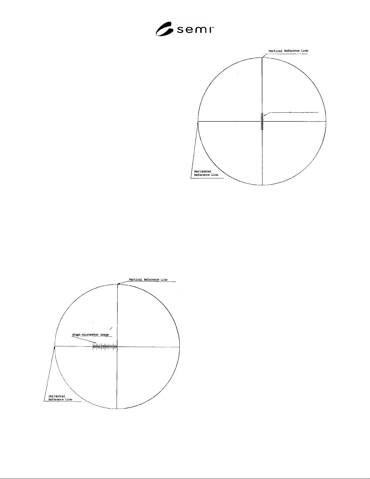
7.1.4 An overlay, with reference lines perpendicular to
each other intersecting at the center, and ten calibrated
divisions on the vertical reference line above and below
center, corresponding to 50 m (0.002 in.) per division at
the sample location. See Figure 1.
NOTE 2: For a 20× overlay, the calibration divisions on the
overlay itself are 1 mm apart.
7.2 Microscope Stage Micrometer — On clear glass or
plastic, the scale to be at least 1.3 mm (0.05 in.) long with
25 m (0.001 in.) divisions.
7.3 Machinists’ Steel Scale — 150 mm (or 6 in.)
minimum length, graduated in 0.50 mm (0.02 in.) or
0.25 mm (0.01 in.).
8 Sampling
8.1 Unless otherwise specified, ASTM Practice E 122
shall be used. When so specified, appropriate sample
sizes shall be selected from each lot in accordance with
ANSI/ASQC Z1.4–1993. Inspection levels shall be
agreed upon between the supplier and purchaser.
9 Calibration
9.1 Comparator Optical Magnification
9.1.1 Place the microscope stage micrometer on the comparator sample stage so that its projected image is at the
center of the viewing screen.
9.1.2 With a steel scale on the viewing screen, count the number of 25 m (0.001 in.) lines projected over a 25 mm
(or 1 in.) distance. Divide the number into 1000 to obtain the actual magnification.
9.1.3 Magnification must be between 19.8 and 20.2 to be usable for this method.
9.2 Comparator Micrometer Travel — x Direction
9.2.1 Set the x-travel micrometer to zero.
9.2.2 Align the projected image of the microscope stage
micrometer such that the array of scale division lines is
horizontal and the right most lines are all to one side of
the vertical reference line on the viewing screen as in
Figure 2.
9.2.3 Using the x-travel micrometer, scan the image of
the microscope stage micrometer until the array has been
transposed to the opposite side of the vertical reference
line in an analogous manner.
9.2.4 Read the x-travel micrometer scale. This value
should agree with the full-range value of the microscope
stage micrometer scale within 25 m (0.001). If the value
does not agree, adjust or repair the micrometer.
10 Procedure
10.1 Mount the overlay (see Figure 1) on the viewing
screen. Position the horizontal reference line
approximately parallel to the floor.
Figure 2
Calibration of the Horizontal Travel
Comparator Stage
Figure 1
Overlay
calibrated divisions
SEMI MF671-0705 © SEMI 2003, 2005 4
10.2 Identify near the horizontal reference line the projected image of a point on the sample stage. A defect or a
particle of dust will serve this purpose. This projected image should be no larger than one-half division on the
overlay scale.
10.3 Align the horizontal reference line to the x-axis travel by repeatedly scanning the point identified in ¶10.2 and
manipulating the overlay and the x-y movement of the sample stage. Alignment is achieved when this point is
centered on the horizontal reference line when scanned from one edge of the viewing screen to the other.
10.4 Place the wafer on the stage so that the central portion of the projected image of the flat is centered on the
viewing screen and is coincident with the horizontal reference line.
10.5 Visually fit the projected image of the flat to the horizontal reference line.
10.5.1 Scan from one end of the flat to the other using the x-axis micrometer.
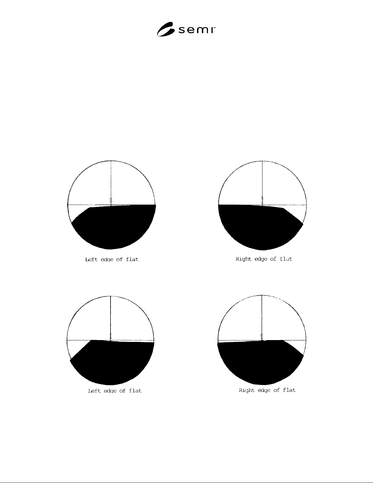
10.5.2 If the apparent shape of the flat is convex, adjust the goniometer and micrometers, while repeating ¶10.5.1
such that the high point is contacting the reference line and the low points are equidistant from the reference line.
See Figure 3.
Figure 3
Aligning a Convex Shaped Flat
10.5.3 If the apparent shape of the flat is concave, adjust the goniometer and micrometers, while repeating ¶10.5.1
such that the high points are contacting the reference line. See Figure 4.
Figure 4
Aligning a Concave Shaped Flat
10.6 Adjust the projected image of the flat using the x-axis micrometer so that the left end is coincident with the
intersection of the vertical and horizontal reference lines.