semi合集-English.pdf - 第7324页
SEMI MF1239-0305 © SEMI 2003, 2005 6 12.2.1.3 If the averag e oxygen reduction values of the group s test ed agree to within a desi red amount, consi d er the groups equi valent. 12.2.2 Method 2 12.2.2.1 Use this method …

SEMI MF1239-0305 © SEMI 2003, 2005 5
A
Apply only to interpretation by Method 2 (see ¶12.2.2).
B
Average and standard deviation of initial O
i
and O
i
reduction apply only to interpretation by Method 1 (see ¶12.2.1).
Figure 1
Suggested Data Sheet Format
12 Calculations and Interpretation of Results
12.1 Subtract each final oxygen concentration value from the corresponding initial oxygen concentration value to
determine the oxygen reduction. Record the oxygen reduction.
12.2 Interpret the results by Method 1 or Method 2 as follows:
12.2.1 Method 1
12.2.1.1 Use this method when the desired target oxygen concentration is already known, when each group tested
has the same target oxygen concentration, and when the range of oxygen concentration values measured in each
group has a range less than 4 ppma (IOC-88). This method cannot be used if the average initial oxygen
concentrations of the groups tested differ by more than 0.5 ppma (IOC-88).
4
12.2.1.2 Determine the averages and standard deviations of the initial oxygen concentration and oxygen reduction
for each group of wafers tested.
SEMI MF1239-0305 © SEMI 2003, 2005 6
12.2.1.3 If the average oxygen reduction values of the groups tested agree to within a desired amount, consider the
groups equivalent.
12.2.2 Method 2
12.2.2.1 Use this method to de-couple oxygen content and precipitation behavior to obtain (1) a qualitative
overview of the precipitation characteristics of the groups tested and (2) the important features of the characteristic
precipitation curve.
12.2.2.2 Bin the oxygen reduction data for each group so that all wafers with oxygen concentration within each 0.5
ppma interval are included in the same bin.
12.2.2.3 Calculate the average of the initial oxygen concentration and the oxygen reduction for each bin in each
group.
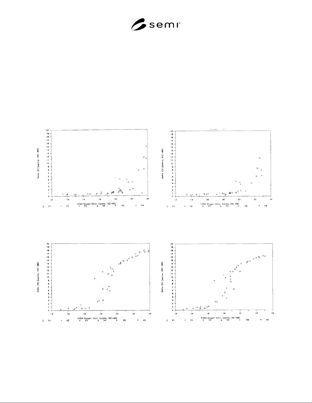
12.2.2.4 Plot the average oxygen reductions against average initial oxygen concentrations for each group tested.
Use a different symbol to distinguish the data for each group. See Figures 2 through 5 for examples of such plots.
Figure 2
Oxygen Reduction in Wafers from Six Groups (V1
to V6) Following Exposure to One-Step Cycle A as
Measured by Laboratory 3
Figure 3
Oxygen Reduction in Wafers from Six Groups (V1
to V6) Following Exposure to One-Step Cycle A as
Measured by Laboratory 4
Figure 4
Oxygen Reduction in Wafers from Six Groups (V1
to V6) Following Exposure to Two-Step Cycle B as
Measured by Laboratory 3
Figure 5
Oxygen Reduction in Wafers from Six Groups (V1
to V6) Following Exposure to Two-Step Cycle B as
Measured by Laboratory 4
12.2.2.5 Note that the curves have three characteristic regions, as illustrated by distinct slope change in Figure 4 and
Figure 5. At low initial oxygen concentration, there is essentially no oxygen reduction; at some value of initial

SEMI MF1239-0305 © SEMI 2003, 2005 7
oxygen concentration, partial precipitation occurs (in this transition region, oxygen reduction changes rapidly with
increasing initial oxygen concentration); at high initial oxygen concentration, full precipitation occurs (in this
region, oxygen reduction is proportional to initial oxygen concentration).
12.2.2.6 Compare the curves obtained for each group. If the data for each group falls within a band of suitable
width, consider the groups equivalent.
13 Report
13.1 Report the following for each group tested:
13.1.1 Identification of group (lot number, location of measurement point on wafer, center or edge, etc.),
13.1.2 Dates of initial and final oxygen measurement and of the heat treatment and identification of operators for
measurement and heat treatment,
13.1.3 Identification of infrared spectrophotometer used,
13.1.4 Table of initial and final oxygen concentrations for each wafer measured, and
13.1.5 Averages and standard deviations of the initial oxygen content and oxygen reduction for each group tested.
13.2 In addition, if Method 2 was used, report the following:
13.2.1 Table of average initial oxygen concentration and average oxygen reduction for each bin in each group, and
13.2.2 Graph of average oxygen reductions against average initial oxygen concentrations for each group.
14 Precision
14.1 Wafers from six different groups with different back surface conditions were processed in two laboratories and
combined. Both Cycles A and B were used. Measurements of initial and final oxygen concentrations on all wafers
tested were made at two other laboratories.
14.2 The wafers within each group did not meet the 2-wafer per 0.5 ppma interval required by these test methods.
14.3 Nevertheless, from the plots reproduced as Figures 2 through 5, both measurement laboratories (that employed
different FT-IR spectrophotometers for making the oxygen determinations at the center of the wafers only)
concluded that the wafers from Groups V1, V3, V4, V5, and V6 were essentially equivalent but those from Group
V2 had increased precipitation in the transition region.
15 Bias
15.1 No reference standards are available for precipitated oxygen, so it is impossible to determine bias except for
that of the individual oxygen measurements. Bias of the individual oxygen measurements should be determined in
accordance with the procedures of the test method utilized.
16 Keywords
delta [O
i
]; interstitial oxygen; oxygen precipitation; oxygen reduction; silicon ; [O
i
]
NOTICE: SEMI makes no warranties or representations as to the suitability of the standards set forth herein for any
particular application. The determination of the suitability of the standard is solely the responsibility of the user.
Users are cautioned to refer to manufacturer's instructions, product labels, product data sheets, and other relevant
literature, respecting any materials or equipment mentioned herein. These standards are subject to change without
notice.
By publication of this standard, Semiconductor Equipment and Materials International (SEMI) takes no position
respecting the validity of any patent rights or copyrights asserted in connection with any items mentioned in this
standard. Users of this standard are expressly advised that determination of any such patent rights or copyrights, and
the risk of infringement of such rights are entirely their own responsibility.
Copyright by SEMI® (Semiconductor Equipment and Materials
International), 3081 Zanker Road, San Jose, CA 95134. Reproduction of
the contents in whole or in part is forbidden without express written
consent of SEMI.