semi合集-English.pdf - 第6524页
SEMI G80-0200 © SE MI 2000 32 A4-1.4.1 The am ount of delay to the input chann el m ust be greater than the inherent delay of the oscilloscope. A4-1.5 A high bandwidth-sa mpling oscilloscop e with statistical calculation…
SEMI G80-0200 © SEMI 200031
APPENDIX 4
NOTE: The material in this appendix is an official part of SEMI G80 and was approved by fulll letter ballot procedures on
September 3, 1999 by the North Amerian Regional Standards Committee.
A4-1 Jitter Measurement
A4-1.1 If a jitter measurement described here is to be
statistically correct the jitter variation in the signal
being measured must be Gausian. The measured jitter
in this method will be represented as one standard
deviation (sigma) of the Gausian distribution, referred
to here as the RMS jitter value.
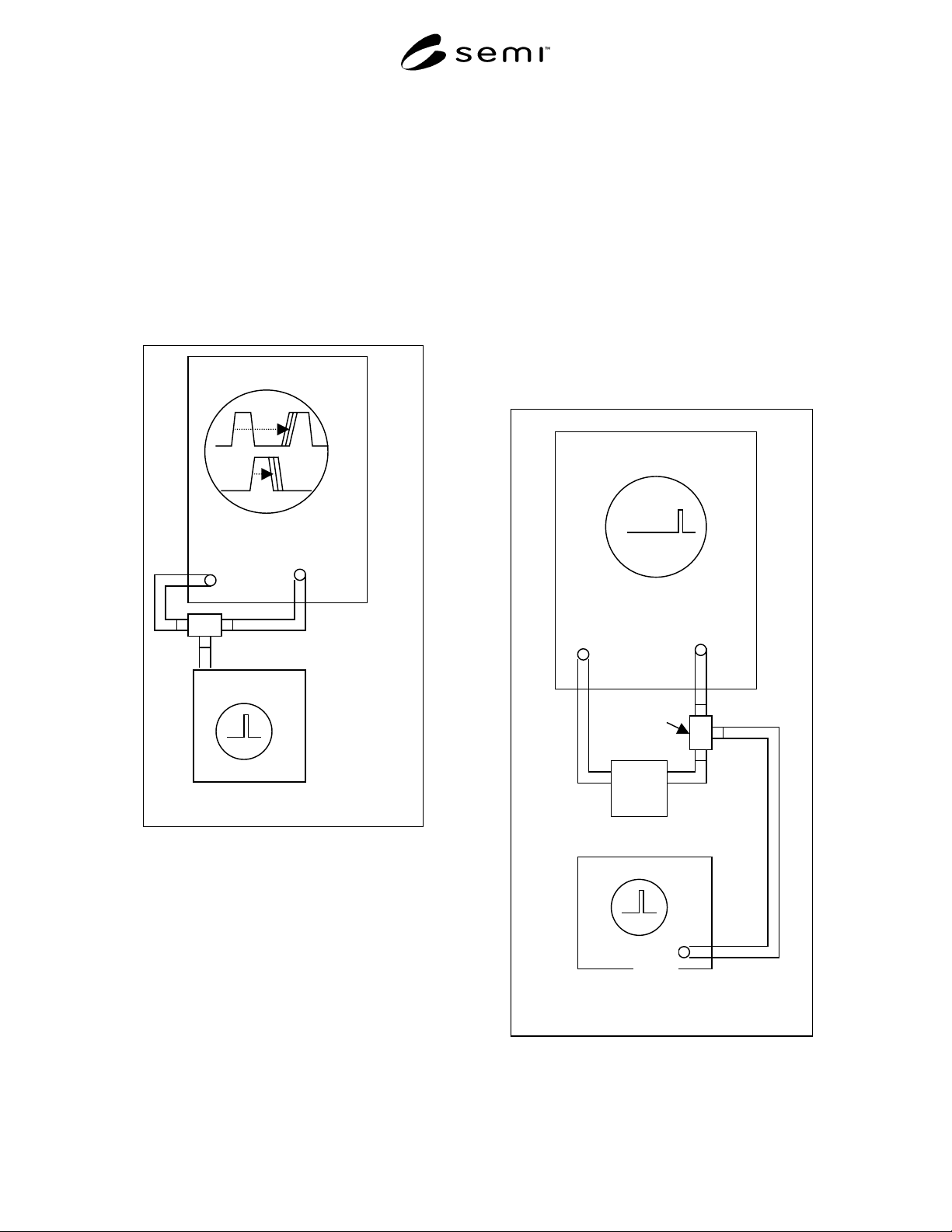
Signal Source
Sampling Oscilloscope
Trigger
Signal
Input
Coax
High frequency power splitter
Figure A4-1
Signal Jitter Measurement
A4-1.2 The signal being measured will have some
amount of jitter. The instrumentation used to measure
the jitter will also have some amount of jitter. To
accurately measure the jitter of a periodic signal the
jitter component of the instrumentation must be
accounted for and subtracted from the signal being
measured.
A4-1.3 Two jitter measurements are required. A jitter
measurement will be made on the signal of interest. A
second jitter measurement will be made to determine
the instrumentation jitter. Instrumentation jitter will be
subtracted from the signal measurement to obtain the
most accurate representation of signal jitter.
A4-1.4 A sampling oscilloscope will have an inherent
delay, typically on the order of 20ns. This represents
the time difference from the time the oscilloscope is
triggered to the time when an input signal can be
viewed. The key to extracting the jitter of the
measurement instrumentation is providing a setup that
allows viewing the trigger on the oscilloscope display.
This is accomplished by delaying the oscilloscope
trigger to an input channel.
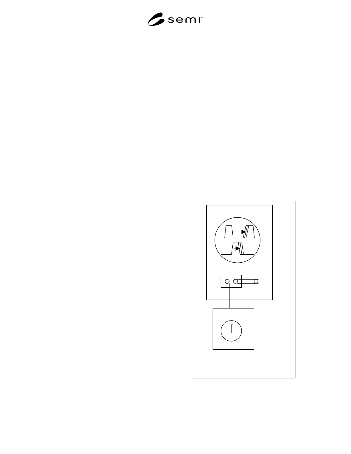
Sampling Oscilloscope
Trigger
Input
Signal
Delay
(Semi-
rigid coax)
High frequency
power splitter
Coax
Pulse Generator
Output
Figure A4-2
Measuring Instrumentation Jitter
SEMI G80-0200 © SEMI 2000 32
A4-1.4.1 The amount of delay to the input channel must
be greater than the inherent delay of the oscilloscope.
A4-1.5 A high bandwidth-sampling oscilloscope with
statistical calculation capability is recommended. In
addition, when making low jitter measurements high
quality RF connectors and cables will be required. A
setup similar to that shown in Figure A4-2 is adequate
for extracting instrumentation jitter.
A4-1.6 Using semi-rigid coax for the delay will
minimize loss of signal. The pulse generator should be
set to low frequency to maximize the pulse width. A
period of 10MHz with a 50ns pulse width is adequate
for an oscilloscope with an inherent delay of 20ns .
The semi-rigid coax length should be chosen to have a
delay slightly larger than the inherent delay of the
oscilloscope. The proper amount of delay allows
viewing the trigger signal with minimal oscilloscope
horizontal delay.
A4-2 Procedure
A4-2.1 A signal measurement will be made as
indicated in Figure A4-1. The semi-rigid coax (delay)
is not used, but the power splitter output will be
connected to the oscilloscope input. As well, the input
to the power splitter is connected to the signal being
measured. The scope is triggered from the input signal,
and the signal being viewed is delayed from the trigger
by an amount equal to the inherent delay of the
oscilloscope. This measurement step provides a value
referred to here as MEASURED RMS SIGNAL
JITTER, MS.
17
A4-2.2 An instrumentation jitter measurement is then
made as indicated in Figure A4-2. Per this arrangement
the signal being displayed is the same signal that
triggered the oscilloscope. That connection scheme
cannot produce any signal jitter between the trigger and
the signal being viewed; thus any jitter shown on the
oscilloscope display represents instrumentation jitter.
This measurement step provides a value referred to here
as MEASURED RMS INSTRUMENTATION JITTER,
MI.
A4-2.3 Since the signal jitter being measured is
Gausian, the sum of squares relationship is used to
subtract out the instrumentation jitter, and thus obtain
ACTUAL RMS SIGNAL JITTER, AS.
MS = (MI
2
+ AS
2
)
1/2
MS- Measured RMS signal jitter.
MI- Measured RMS instrumentation jitter.
AS- Actual RMS signal jitter.
17 Use of a loop-through sampling head is an alternative method for
making this measurement.
A4-3 Example
A4-3.1 Measured RMS signal jitter MS, the signal
being measured, results in a 10ps measurement.
A4-3.2 Measured RMS instrumentation jitter MI, the
jitter of the measurement setup, results in a 5ps
measurement.
A4-3.3 The actual RMS signal jitter AS is determined
from the relationship:
MS = MI
2
+ AS
2
)
1/2
and calculates to be:
10
2
= 5
2
+ AS
2
100 = 25 + AS
2
75 = AS
2
75
1/2
= AS
8.66ps = AS (actual RMS signal jitter)
Since the jitter is Gaussian, the max value of jitter is
approximately equal to 5 or 6 times the RMS value of
the jitter.
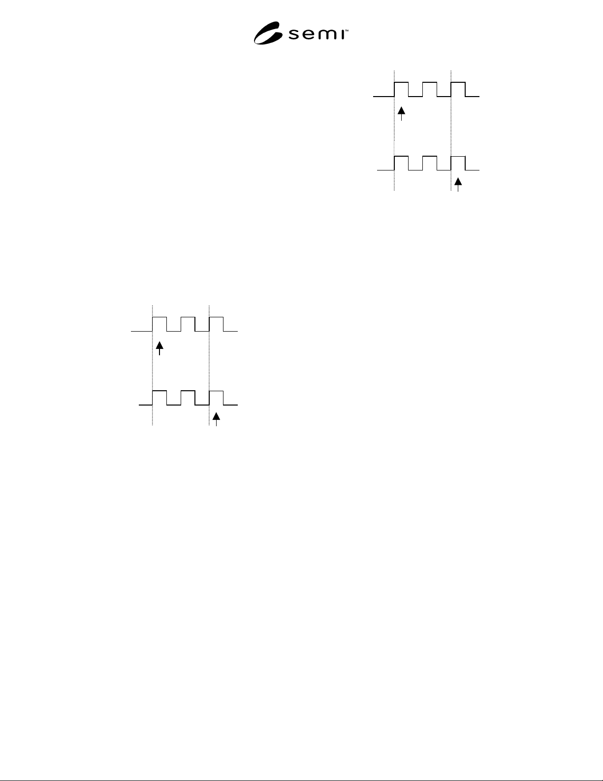
Signal Source
Sampling Oscilloscope
Trigger
Loop through head
In Out
Figure A4-3
Use of a Loop-Through Sampling Head
SEMI G80-0200 © SEMI 200033
A4.4 Use of a Loop-Through Sampling Head
A4-4.1 This is an alternate approach to measured RMS
signal jitter. The input signal is routed through the loop-
through sampling head where it is sampled and sent to
the output of the sampling head. The head output is
connected to the oscilloscope trigger. (See Figure A4-
3.)
A4-4.2 What is Observed When Making MS And MI
Measurements — This dialog is meant to provide
further clarification for making jitter measurements.
This is an example that applies to a jitter measurement
using an oscilloscope with an inherent oscilloscope
delay of 20ns. The signal frequency is 100MHz (period
of 10ns ). The semi-rigid coax delay is set to the
inherent oscilloscope delay of 20ns.
A4-4.3 Measured RMS Signal Jitter, MS — For the
MS measurement the observed edge occurs subsequent
to the edge that triggered the oscilloscope:
N
N
+1
N
+2
N
+2
This pulse triggers the oscilloscope.
Observed Edge –– The pulse that is
displayed on the oscilloscope is not the
same pulse that triggered the oscilloscope.
Trigger:
Signal:
Figure A4-4
Measured RMS Signal Jitter, MS
A4-4.4 The observed edge depends upon the signal
frequency; thus what is displayed is subsequent to the
trigger pulse permitting signal jitter to be observed.
A4-4.5 Measured RMS Instrumentation Jitter, MI —
For the MI measurement the observed edge is the same
edge that triggered the oscilloscope.
N
–1
N
+1
N
+2
N
This pulse triggers the oscilloscope.
Observed Edge –– The pulse that is
displayed on the oscilloscope is the same
pulse that triggered the oscilloscope.
N
–2
Trigger:
Signal:
Figure A4-5
Measured RMS Instrumentation Jitter, MI
A4-4.6 There is no repetitive aspect of the signal, thus
whatever jitter you observe is strictly instrumentation
jitter.
A4-4.7 Summary –– Jitter is only observable for a
periodic signal or repetitive edge. Thus when MS
measurements are made signal jitter is observed
because a subsequent or repetitive signal is displayed
(in addition to instrumentation jitter). When MI
measurements are made the input signal is delayed such
that you see the same edge that trigger the oscilloscope.
That creates a non-repetitive or non-periodic occurrence
of the observed signal, thus the jitter observed is strictly
due to the instrumentation.
NOTICE: SEMI makes no warranties or
representations as to the suitability of the standards set
forth herein for any particular application. The
determination of the suitability of the standard is solely
the responsibility of the user. Users are cautioned to
refer to manufacturer’s instructions, product labels,
product data sheets, and other relevant literature
respecting any materials mentioned herein. These
standards are subject to change without notice.
The user’s attention is called to the possibility that
compliance with this standard may require use of
copyrighted material or of an invention covered by
patent rights. By publication of this standard, SEMI
takes no position respecting the validity of any patent
rights or copyrights asserted in connection with any
item mentioned in this standard. Users of this standard
are expressly advised that determination of any such
patent rights or copyrights, and the risk of infringement
of such rights, are entirely their own responsibility.
Copyright by SEMI® (Semiconductor Equipment and Materials
International), 3081 Zanker Road, San Jose, CA 95134. Reproduction o
f
the contents in whole or in part is forbidden without express written
consent of SEMI.