semi合集-English.pdf - 第4560页
SEMI D28-1101 © SEMI 2001 4 Table 1 Substrate Edge Length, Interface Dime nsions, and Toleranc es Interfac e Dim ensio ns and Tolerances[ mm] Substr ate Edge Length [ mm] X1 max. X2 max. X3 max. Y1 max. Y2 max. Y3 max. Z…
SEMI D28-1101 © SEMI 20013
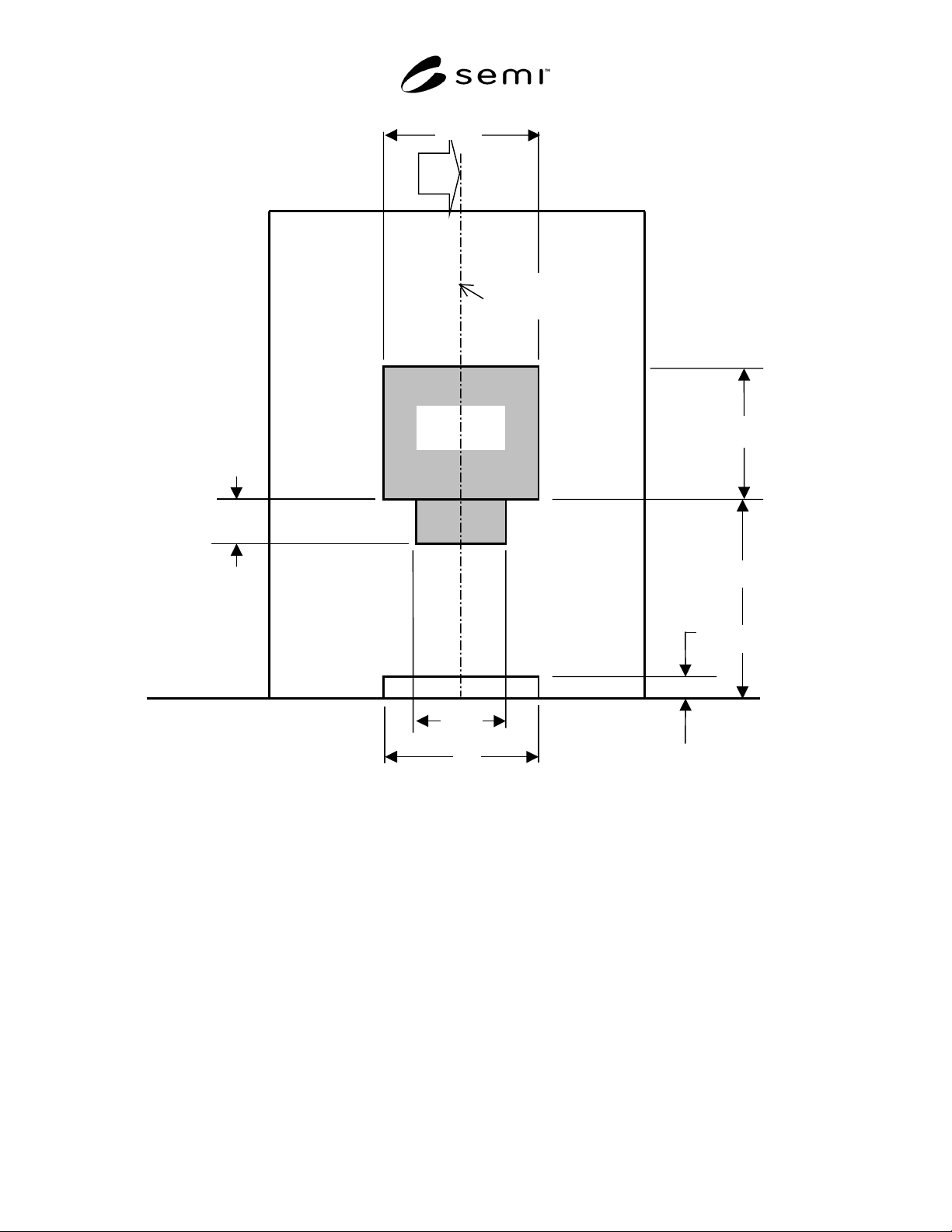
X1
Z1
Z4
X2
Z5
Exclusion
Zone
Vertical
Datum Plane
Z2
A
X
3
Figure 1B
Front View of Tool port
SEMI D28-1101 © SEMI 2001 4
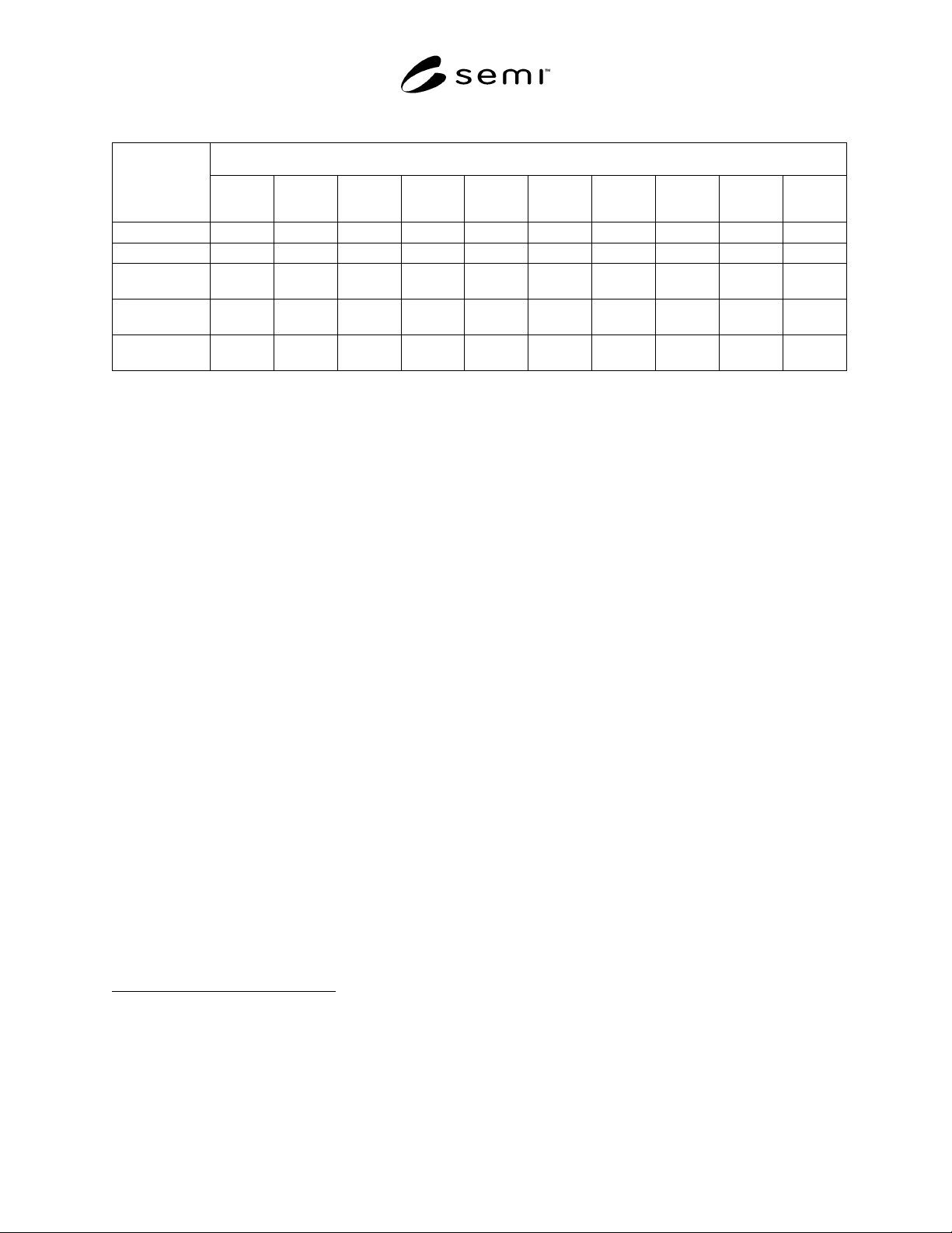
Table 1 Substrate Edge Length, Interface Dimensions, and Tolerances
Interface Dimensions and Tolerances[mm]
Substrate Edge
Length [mm]
X1
max.
X2
max.
X3
max.
Y1
max.
Y2
max.
Y3
max.
Z1
± 2 mm
Z2
max.
Z4
max.
Z5
max.
550 × 650
925 450 600 500 440 130 900, 950 1000 150 250
600 × 720
980 500 600 535 475 130 900, 1000 1000 150 250
680 × 880
1100 560 600 615 565 130
1000,
1100
1000 150 300
730 × 920
1150 600 600 630 590 130
1000,
1100
1000 150 300
800 × 950
1200 660 600 650 605 130
1000,
1100
1000 150 300
NOTE 1: Two values are specified for Z1, either value can be chosen.
8 Related Documents
8.1 SEMI Standards
SEMI D5 — Standard Size for Flat Panel Display
Substrates
SEMI D11 — Specification for Flat Panel Display
Glass Substrate Cassettes
SEMI D16 — Specification for Mechanical Interface
Between Flat Panel Display Material Handling System
and Tool Port
8.2 Semiconductor Equipment Association of Japan
(SEAJ)
Semiconductor Equipment Association of Japan (SEAJ)
Liquid Crystal Display Manufacturing Equipment
Standardization Guideline – for Glass Substrate Size
800 × 950 (SEAJ/P-S3005-98, SEAJ/P-S3006-98), June
1998
1
8.3 SEMI PCS-FPD
SEMI PCS-FPD — Production Cost Saving (PCS)
Forum – FPD Phase III Report, June 1999
2
NOTICE: SEMI makes no warranties or
representations as to the suitability of the standards set
forth herein for any particular application. The
determination of the suitability of the standard is solely
the responsibility of the user. Users are cautioned to
refer to manufacturer’s instructions, product labels,
1 Semiconductor Equipment Association of Japan, 7-10, Shinjuku 1-
chome, Shunjuku-ku, Tokyo, 160-0022 Japan, tel:+81-3-3353-7589,
fax:+81-3-3353-7970, http://www.seaj.or.jp
2 SEMI PCS-FPD Production Cost Saving (PCS) Forum – FPD
Phase III Report, June 1999, Semiconductor Equipment and
Materials International, 3081 Zanker Road , San Jose, CA 95134-
2127 U.S.A.tel.+1-408-943-6900 fax:+1-408-428-9600
http://www.semi.org
product data sheets, and other relevant literature with
respect to any materials mentioned herein. These
standards are subject to change without notice.
The user’s attention is called to the possibility that
compliance with this standard may require use of
copyright material or of an invention covered by patent
rights. With publication of this standard, SEMI takes no
position in respect to the validity of any patent rights or
copyrights asserted in connection with any item
mentioned in this standard. Users of this standard are
expressly advised that determination of any such patent
rights or copyrights, and the risk or infringement of
such rights, are entirely their own responsibility.
SEMI D28-1101 © SEMI 20015
RELATED INFORMATION 1
ASSUMED DIMENSIONS FOR SUBSTRATE EDGE AND CASSETTE
SIZE
NOTE: This related information is not an official part of SEMI D28 and was derived from work of the originating
committee. This related information was approved for publication by full letter ballot procedures on August 3,
2001.
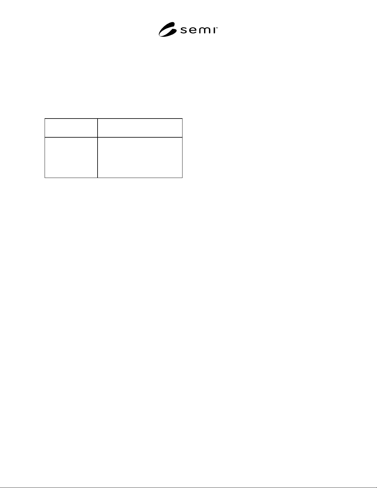
Table R1-1 Cassette Size
Substrate Edge
length [mm]
Cassette size [mm]
Width×Length×Height
550 × 650
600 × 720
680 × 880
730 × 920
800 × 950
591 × 682 × 524
642 × 755 × 695
736 × 923 × 706
792 × 978 × 770
870 × 1010 × 810
NOTE 1: 550 × 650, 600 × 720, 680 × 880, and 730 × 920 are the
sizes which are actually adopted at the manufacturing sites. As for
800 × 950, please refer to SEMI PCS-FPD-Phase III Report.
NOTE 2: Cassette sizes in Table R1-1 were used only hypothetically
as assumption to prescribe dimensions in Table 1.
NOTICE: SEMI makes no warranties or
representations as to the suitability of the standards set
forth herein for any particular application. The
determination of the suitability of the standard is solely
the responsibility of the user. Users are cautioned to
refer to manufacturer's instructions, product labels,
product data sheets, and other relevant literature,
respecting any materials or equipment mentioned
herein. These standards are subject to change without
notice.
By publication of this standard, Semiconductor
Equipment and Materials International (SEMI) takes no
position respecting the validity of any patent rights or
copyrights asserted in connection with any items
mentioned in this standard. Users of this standard are
expressly advised that determination of any such patent
rights or copyrights, and the risk of infringement of
such rights are entirely their own responsibility.
Copyright by SEMI® (Semiconductor Equipment and Materials
International), 3081 Zanker Road, San Jose, CA 95134. Reproduction o
f
the contents in whole or in part is forbidden without express written
consent of SEMI.