semi合集-English.pdf - 第6470页
SEMI G78-0699 © SE MI 1999 3 5.17 scrub mark — m a r k l e f t b y t h e p r o b e i n t h e bondin g pad or bum p after the probe card h as touched down on t he wafer. 5.18 te mperatur e testi ng — testi ng o f de vice …
SEMI G78-0699 © SEMI 1999 2
pads or interconnect bumps on a semiconductor device
to a set of test needles attached to a probe card.
5.4 bonding pad — exposed metal lic contact area on a
semiconductor device that is surrounded by dielectric
passivation. This is the point at which a temporary
interconnect is made for wafer level test, and permanent
interconnect for packaging.
5.5 bumps — metallic elevated co ntact area on a
semiconductor device that is used in place of a bonding
pad. A die that is designed to use this type of
connection is commonly called a ‘flip chip’ or direct
chip attach.
5.6 die — individual semiconduct or device. For the
purposes of this method, the dice have not been
singulated, and are still in the form of a wafer. Used
interchangeably (in the context of wafer sort) with the
acronym DUT (Device Under Test).
5.7 overdrive — distance in Z whi ch the wafer is
driven beyond a user defined initial contact point,
typically ‘first electrical contact’.
5.8 overhead test — semiconducto r test method where
the test head is mounted directly over the prober, with
the goal of shortening the distance between the pin
electronics and the probe card. The connection
between the test head and the prober is generally
through a device called a Prober Tester Interface (PTI)
5.9 pin electronics — tester hardware that creates the
test signals used to challenge the DUT.
5.10 probe card — printed wiring b oard or ceramic
substrate with permanently attached needles or contacts
that are aligned at the time of manufacture to match the
contact pattern on a Die. Common types of probe cards
are:
• Blade
• Peripheral / Cantilever (AKA Epoxy Ring)
• Vertical (AKA Area Array or Cobra™)
5.11 probe card planarity and alignment — a user-
specified position of the probe tips in ‘x’, ‘y’ and ‘z’.
5.12 probe needles — the contact p oints between the
probe card and the bonding pads. These are typically
manufactured from one of the following materials:
• Beryllium copper
• Tungsten
• Tungsten-rhenium alloy
• Paliney
5.13 prober tester interface (PTI) — signal-
transmitting electro-mechanical device that connects
the pin cards in the tester to the probe card.
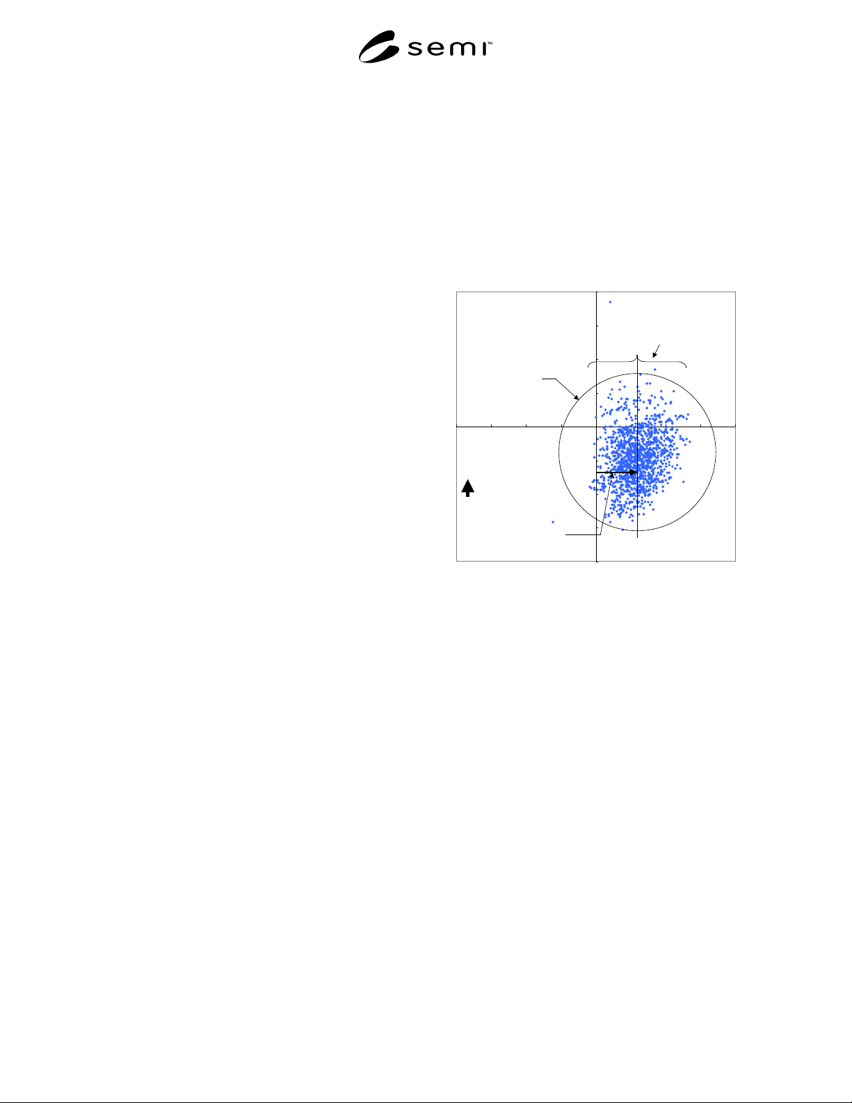
5.14 repeatability — Figure 1 is em pirical data and
represents a statistically significant sample of scrub
marks. This data reveals that probe needles may not
make contact consistently to the same point die to die.
Recall that accuracy is defined in this method as
average die offset. Thus, repeatability simply represents
the three-sigma distribution value for average die offset.
Repeatability will represent 99.7% or a three-sigma
distribution value for the accumulated offset data points
obtained through use of this method.
-20
-15
-10
-5
0
5
10
15
20
-20 -15 -10 -5 0 5 10 15 20
microns
microns
Repeatability
A
ccuracy
Average
approximation of
data points
Raw X-data
Direction of the
probe needle
Figure 1
Raw X-Data
5.14.1 The X-Y plotted centroids of these scrub marks
will be found to form a “cloud” of points, densest in the
center, and thinning out towards the edges.
5.14.2 Repeatability is the radius of th at cloud or
“cluster” of probe marks, as defined by the 3 σ or other
user defined limit of that cloud. The error in the
placement of the center of that cloud, relative to its
nominal target, is defined as the automatic wafer
prober’s “Accuracy”. (See Figure 1)
5.15 set point — the value to which a control system’s
input device has been set, as opposed to the actual value
to which the control system has driven the controlled
variable. For example, the input setting to the wafer
chuck temperature controller, as opposed to the actual,
independently measured temperature of the wafer
chuck.
5.16 soak time — time between a piece of equipment’s
reaching the set point temperature and use of that piece
of equipment.

SEMI G78-0699 © SEMI 19993
5.17 scrub mark — mark left by the probe in the
bonding pad or bump after the probe card has touched
down on the wafer.
5.18 temperature testing — testing of devices at a
controlled temperature level other than ambient.
5.19 test — one complete run-throu gh of the data
collection portion of this document on one automated
wafer prober.
5.20 tester — specialized computer controlled system
designed to test integrated circuits.
5.21 prober communications protocol (see Section
9.6) — means of transmitting data between the tester
and the prober. Common methods are:
• TTL
• RS-232c
• GPIB
5.22 test head — package of electronics (part of the
Tester) which interacts both electrically and
mechanically with the probe card, typically through the
Prober Tester Interface (PTI).
5.23 throughput — rate at which die can be cycled, by
the automatic wafer prober, for the purpose of being
tested. It is inherent in the functionality of an automatic
wafer prober (or any other motorized positioning
device) that accuracy, repeatability and throughput are
intimately and inseparably related.
5.24 touch down — contact between the probe card
and the wafer. This user may choose to define this as
either first electrical or first mechanical contact.
5.25 wafer — semiconductor substrate upon which
multiple die are fabricated.
5.26 wafer boat or wafer cassette — carrier for
multiple wafers.
5.27 wafer chuck — platform withi n an automatic
wafer prober that supports and transports the wafer.
The chuck may contain the means for controlled
temperature testing.
5.28 x, y, z and
θ
— motions relativ e to the center of
the Probe Card when standing in front of the Prober:
• Motion to the right is motion in the positive X-
direction.
• Motion towards the back of the prober is motion in
the positive Y-direction.
• Motion away from the floor is the positive Z-
direction.
• Motion revolving around a Z-axis passing through
the center of the probe card is θ-motion. Motion in
the counter-clockwise direction when facing down
from above the prober is motion in the positive θ-
direction.
5.29 z-clearance — distance between the user defined
initial contact point and the top surface of the wafer
during that portion of the wafer prober’s cycle when the
wafer chuck is moving the wafer between DUTs.
6 Summary of Method
6.1 Objective – A SEMI Probe Sta ndards Task Force
has defined this method. That task force consisted of
members from semiconductor wafer probe system users
and wafer probe system suppliers. This method, in part
a guide to collection of data, is aimed at a specific set of
wafer probe system parameters: accuracy, repeatability
and throughput. This method is a tool that creates
comparative data. That data will act as a criterion by
which multiple wafer probe systems can be judged
competitively.
6.2 Probe System Accuracy and Throughput – A wafer
probe system will have needle placement error due to
the probe system electromechanical systems, and
additional needle placement error due to the probe card
physical alignment of the needles. The degree of
accuracy to which the probe system can place the
chuck, the effectiveness of the probe system's bond pad
to needle alignment, the physical alignment of the
probe card needles in their X and Y plane, and the
probe system's vision resolution and accuracy (x
microns of distance per pixel) will be the factors that
influence a probe system's overall placement
performance.
6.2.1 Probe system comparative acc uracy and
repeatability are established in this method using probe
mark data acquired manually with a vision system or, if
available, through use of an automated probe mark data
analysis system. Acquired data is analyzed with the
Probe Mark Data Analysis algorithm contained in this
method.
6.2.1.1 The intention of this data colle ction exercise is
not to make a deterministic conclusion establishing a
probe system’s accuracy. Data analysis results are only
meaningful in the context of a comparative analysis of
multiple probe systems.
6.2.2 Probe system throughput is be st determined
using time measurements made using a stopwatch.
Other approaches can be applied, such as:
• the time stamp and log file (if available) on the
probe system under evaluation.
• time tracking within the device test program
employed for testing the prober.
6.2.3 Any of these approaches is via ble for measuring
time intervals during probe system operation. That data

SEMI G78-0699 © SEMI 1999 4
is to be entered into the data collection table as part of
the application of this method.
6.2.4 The algorithm collects data from 9 wafers out of
a lot of 10. Three setups are performed using 3 wafers
per setup. All dice will be probed, but data will be taken
only on twelve of the die on each wafer. Twenty-four
pads on each die are evaluated (see Figure 4). Overall,
2592 die pads are analyzed in a lot.
6.2.5 When all the data is collected and analyzed, each
probe system will have an average die offset value.
This will be a comparative representation of accuracy
consisting of average offsets for all evaluated die. This
comparative representation of accuracy is a measure of
how accurate the probe systems place the chuck, and
thus the probe needles, to the center point on the die
pads, consistent with normal operation of the probe
systems.
6.2.6 In general, when the probe marks are viewed
across all dice, there will be a data spread, or
distribution of error points for each wafer.
Repeatability is the ± 3σ variation of all die offsets,
identified in this method as the 3σ calculation of
Normalized Die Offset.
6.3 Probe Card Issues – Probe card construction
variability and probe card usage at temperatures other
than ambient are important considerations. The
following sources of error should be kept in mind:
• In a hot chuck environment the probe card and
needles will experience a high percentage of the
elevated chuck temperature. The material selection
for the probe card will determine how it expands
and contracts due to the temperatures applied.
Probe systems can be equipped with programmable
preheat (soak) times. Longer preheat times will
reduce probe card variability while decreasing
throughput.
• Needle construction can result in excessive error
due to bending of the needles when excessive
probe system z-stage overdrive is applied. The
number of needles and the selection of needle
technology, i.e., cantilever versus vertical, is
another variable, having a noticeable influence on
measurement results.
• Since each user of this method is not confined to a
standard for probe card construction, the user of
this method is advised to choose a probe card and
vendor with good integrity, and to use that same
probe card when evaluating multiple probe
systems. The assertion here is that the same probe
card used to evaluate multiple systems will react in
a repeatable manner under varying environmental
conditions. This assumes there is no excessive
probe card needle wear during the multiple
evaluations, and that needle alignment is verified
or achieved before each execution of the
procedure.
6.3.1 Probe mark scrub length can vary due to several
factors including:
variations in the flatness of the chuck and
stage travel that are not compensated by the z-
sensor mapping algorithms
by hard spots in the aluminum pads, or
by variations in probe tip geometry, etc.
6.3.2 To minimize the impact of this variation in the
probe mark analysis algorithm, use only scrub mark
location data that is taken normal to the direction of
scrub. Distances measured normal to the orientation of
the scrub mark are generally accepted to be
significantly more stable than that which is taken
parallel to the scrub mark (see Figure 2).
6.3.3 In summary, the probe card itself can be a
limiting factor when making needle placement accuracy
measurements, especially at varying environmental
conditions. Material selection, vendor to vendor
variation, construction of a probe card (blade, epoxy
ring, vertical, etc.), especially with varying
environmental conditions, will create inconsistent
analysis results, unless care is taken with the
application of this method. The precautions discussed
here are meant to promote consistent and accurate
evaluation results for this method.
6.3.4 Nevertheless, the precautions mentioned here
could ALSO be an important basis for using this
method. As an example, a probe card is typically
designed for XY positional placement and planarity,
and is expected to meet customer specification
requirements in normal operation at room temperatures.
This method could serve as a means of establishing
numerical results that represents the effects that
temperature or probe card construction variability have
on probe card specification requirements.
6.4 The PMA Algorithm – A best-f it rectangle can be
drawn around the scrub mark and the passivation
opening for each pad, reference Figure 3.
NOTE: Applying a best-fit rectangle around the passivation
opening may prove difficult for certain vision systems.
Application of the best-fit rectangle around the die pad metal
is an acceptable alternative. The center position of the best-fit
rectangle around the scrub mark will represent the center of
the scrub mark. The center of the die pad is the center of the
best—fit rectangle around the passivation opening. The
distance between the two centers is the pad offset. Pad offset
is computed from the four values left, right, top, and bottom,
reference Figure 2.