semi合集-English.pdf - 第6399页
SEMI G72.2-099 7 © SEMI 1997 12 *5. Th ermal en hancemen t of 6 x 6 sold er ba lls. NOTICE: These st andards do not purport to addres s safety issues, if any, ass o ciated with their use. It is the responsibility of t he…
SEMI G72.2-0997 © SEMI 199711
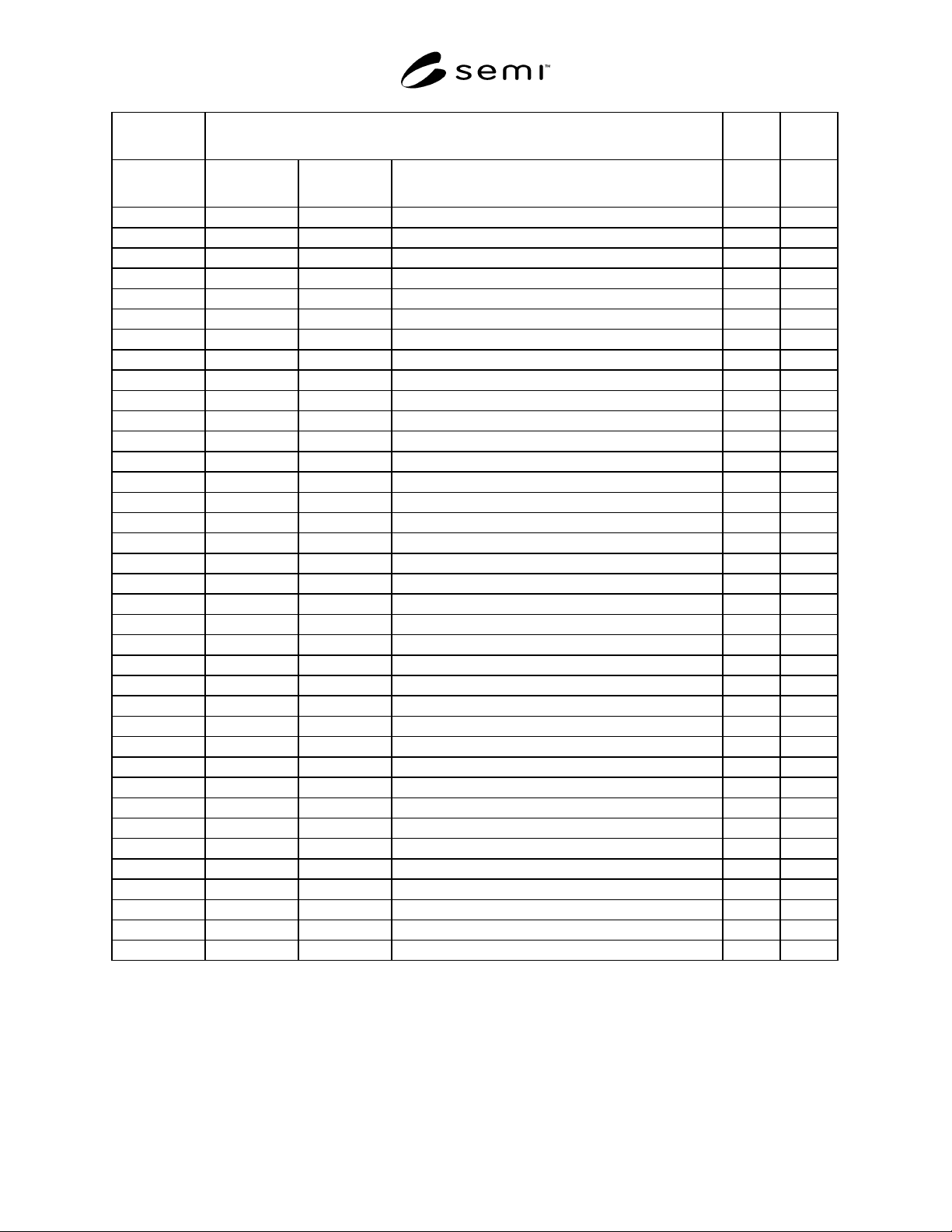
Design
No.PBD0002 SEMI Standard BGA Design Library Revision Initial
Date
10/22/96
Page
2 of 10
PBGA Wire
Bond Pad (*1)
Solder Ball
Location
Die Wire Bond
Pad (*3) I/O Name (& Comments) (*4)
Pkg.
Side (*1) Notes
121 AE16 2
125 AE17 2
129 AE18 2
132 AE19 2
135 AE20 2
139 AE21 2
143 AE22 2
146 AE23 2
150 AE24 2
w/b ring 1 AE25 3
153 AE26 3
w/b ring 1 AF1 3
77 AF2 2
79 AF3 2
82 AF4 2
86 AF5 2
90 AF6 2
92 AF7 2
96 AF8 2
99 AF9 2
102 AF10 2
106 AF11 2
108 AF12 2
112 AF13 2
116 AF14 2
120 AF15 2
123 AF16 2
127 AF17 2
131 AF18 2
133 AF19 2
137 AF20 2
141 AF21 2
144 AF22 2
148 AF23 2
152 AF24 2
w/b ring 1 AF25 3
w/b ring 1 AF26 3
NOTES:
*1. Please refer to Notes column for explanations of wirebond (w/b) rings. PBGA Wirebond Pads are numbered counter clockwise, starting with
Pad #1 in the upper left hand corner. Please refer to Top View of package for package side #1, 2, 3, or 4 (Figure 1).
*2. Metallized wirebond (w/b) ring 2 surrounds die attach area for wirebonding to electrically common die pads and electrical connection with
solder balls designated by 2nd Electrical Group symbol on BGA Design Library Drawing (Figure 1).
*3. Metallized wirebond (w/b) ring 1 surrounds die attach area for wirebonding to electrically common die pads and electrical connection with
both die attach pad and solder balls designated by 1st Electrical Group symbol on BGA Design Library Drawing (Figure 1).
*4. If the number of signal Die Wirebond Pads (not including Electrical Groups) total less than 304, the total number may be divided by 4 and
wirebond placement centered on each package side.

SEMI G72.2-0997 © SEMI 1997 12
*5. Thermal enhancement of 6 x 6 solder balls.
NOTICE: These standards do not purport to address
safety issues, if any, associated with their use. It is the
responsibility of the user of these standards to establish
appropriate safety and health practices and determine
the applicability of regulatory limitations prior to use.
SEMI makes no warranties or representations as to the
suitability of the standards set forth herein for any
particular application. The determination of the
suitability of the standard is solely the responsibility of
the user. Users are cautioned to refer to manufacturer’s
instructions, product labels, product data sheets, and
other relevant literature respecting any materials
mentioned herein. These standards are subject to
change without notice.
The user’s attention is called to the possibility that
compliance with this standard may require use of
copyrighted material or of an invention covered by
patent rights. By publication of this standard, SEMI
takes no position respecting the validity of any patent
rights or copyrights asserted in connection with any
item mentioned in this standard. Users of this standard
are expressly advised that determination of any such
patent rights or copyrights, and the risk of infringement
of such rights, are entirely their own responsibility.
Copyright by SEMI® (Semiconductor Equipment and Materials
International), 3081 Zanker Road, San Jose, CA 95134. Reproduction o
f
the contents in whole or in part is forbidden without express written
consent of SEMI.
SEMI G73-0997 (Reapproved 1104)
TEST METHOD FOR PULL STRENGTH FOR WIRE BONDING
This test method was technically approved by the Global Assembly & Packaging Committee and is the direct
responsibility of the Japanese Packaging Committee. Current edition approved by the Japanese Regional
Standards Committee on July 23, 2004. Initially available at www.semi.org September 2004; to be published
November 2004. Originally published in 1997.
1 Purpose
1.1 This standard defines the pull strength test method
for wire bonding.
2 Scope
2.1 This standard defines the destructive pull strength
test method and its criterion for evaluating pull strength
of wire bonds connecting two points, connected by
using ball bonding technique.
2.2 This standard can be applied to measure wires
whose diameter is less than 100 microns.
NOTICE: This standard does not purport to address
safety issues, if any, associated with its use. It is the
responsibility of the users of this standard to establish
appropriate safety and health practices and determine
the applicability of regulatory or other limitations prior
to use.
3 Referenced Standards
3.1 Military Standard
1
MIL-STD-883D — Test Methods and Procedures for
Microelectronics
NOTICE: Unless otherwise indicated, all documents
cited shall be the latest published versions.
4 Terminology
4.1 Definitions
4.1.1 hook — L or similar-shaped tool for hooking a
wire for pull test.
5 Apparatus
5.1 Pull Tester or equivalent equipment
5.1.1 Enough stroke to break a wire.
5.1.2 Accuracy — Within ± 0.5% to the full scale of
load cell.
5.1.3 Pull Speed — Constant speed.
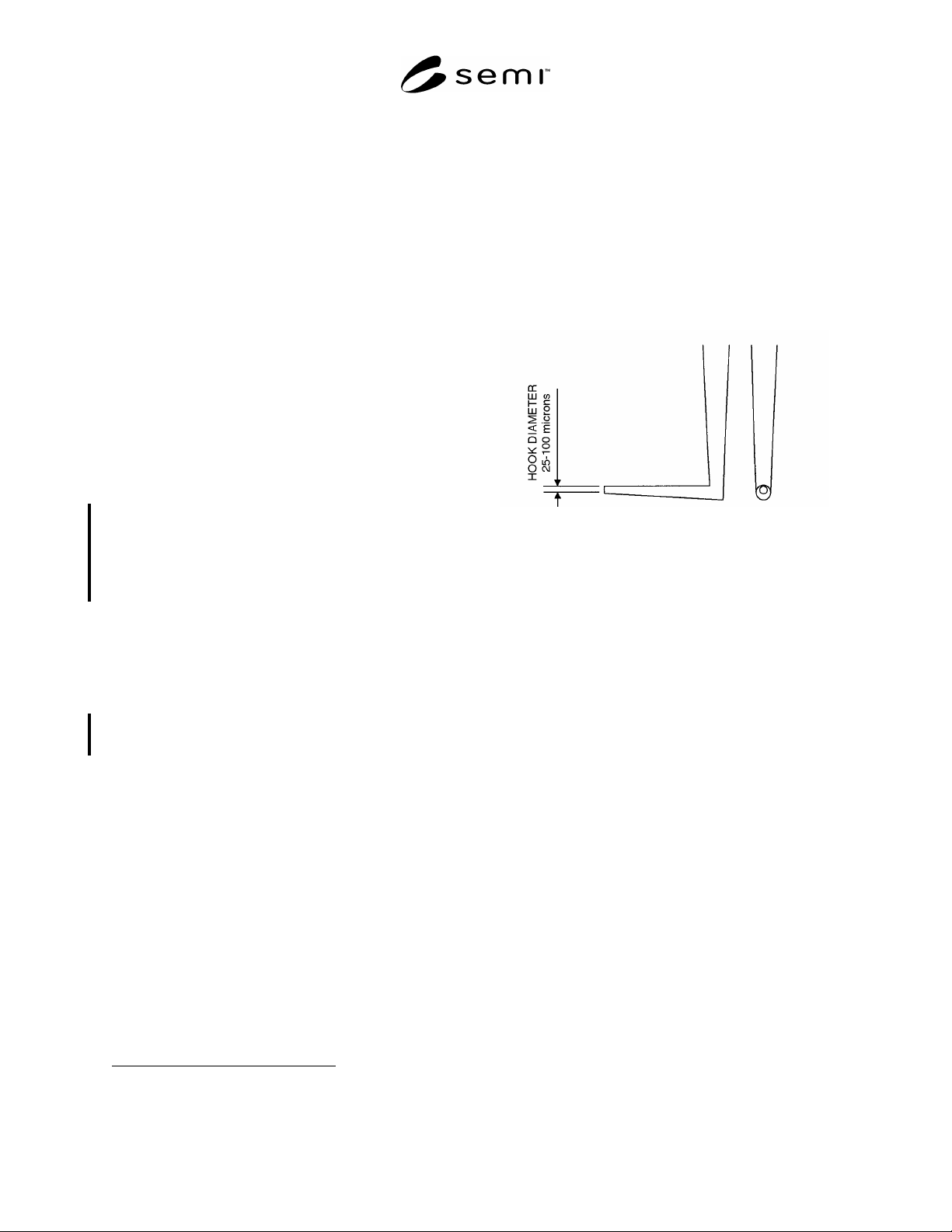
5.1.4 Hooks — Between 25–100 microns in diameter.
1 United States Military Standards, Available through the Naval
Publications and Forms Center, 5801 Tabor Avenue, Philadelphia,
PA 19120-5099, USA. Telephone: 215.697.3321
NOTE 1: Hook must be made of material strong enough to
break wire while testing but not with a small diameter so as to
cut through the wire.
Figure 1
Hook Diameter
5.1.5 Calibration of equipment must be simple enough
so that users can calibrate it easily. Instructions for
calibration should be described in equipment manual.
6 Sampling
6.1 Measure at least 30 points from at least 2 devices.
From each side of the devices, select the same number
of wires randomly.
7 Calibration and Standardization
7.1 Calibration Method
7.1.1 Calibration of equipment should be done using
official and traceable weights.
7.1.2 Display the weight and verify whether the results
are within the equipment’s accuracy.
7.1.3 Repeat the measurement using other weights to
verify repeatability and linearity of the calibration.
7.2 Interval of Calibration
7.2.1 Calibrate at regular intervals at least once a year.
7.2.2 Calibration must be able to be done just before
testing when necessary or specifically instructed.
1 SEMI G73-0997 © SEMI 1997, 2004