semi合集-English.pdf - 第6185页
SEMI G39-89 © SEMI 198 6, 1989 1 SEMI G39-89 SPECIFICA TION FOR BRAZED LEAD FLATPACK CONSTRUCTIONS, INCLUDING LEADFRA M ES, SUITA BLE FOR AUTOM A TED A SSEMBLY 1 Preface This specification defines the s tandard requireme…
SEMI G38-0996 © SEMI 1987, 2004 9
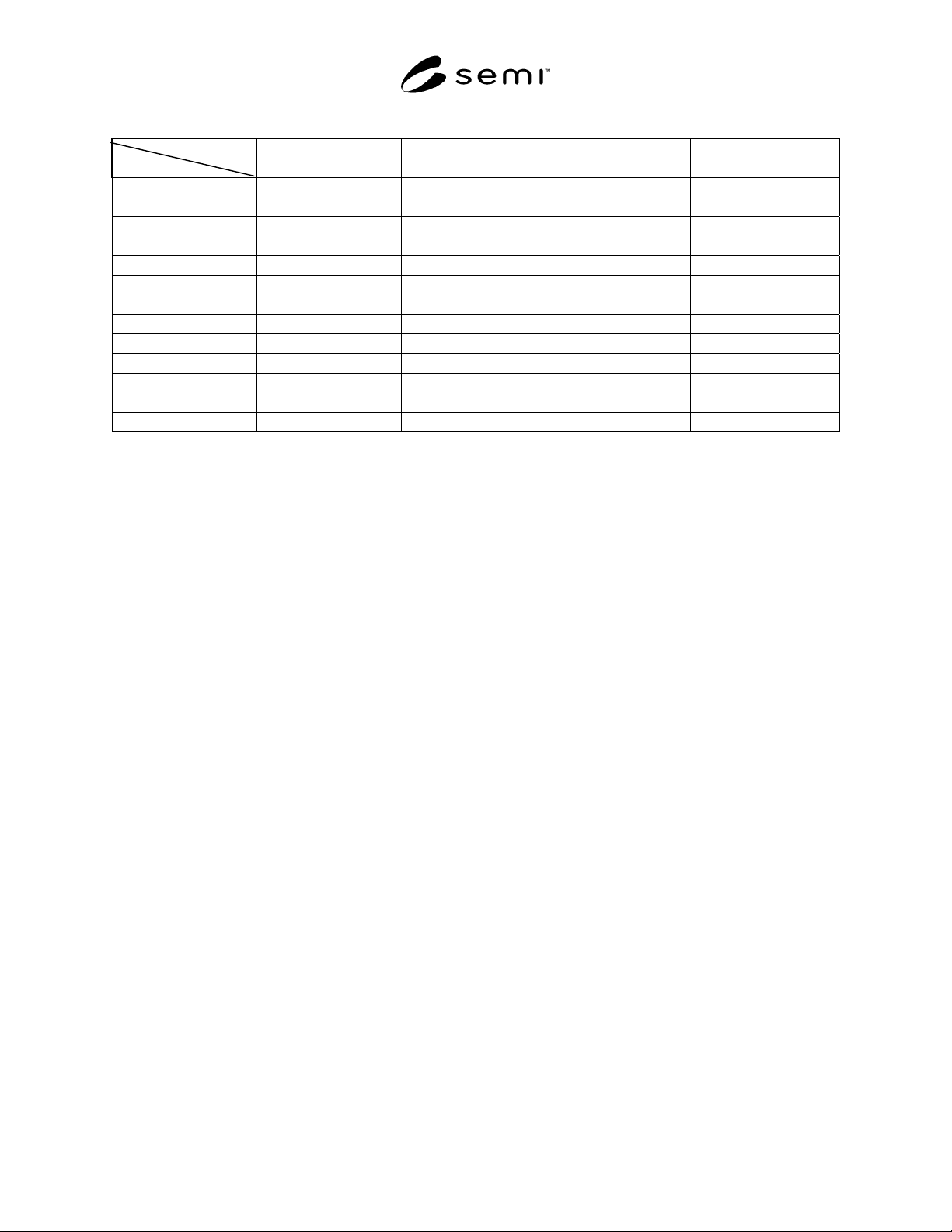
Units: °C/W
Air Velocity (m/s)
Sample No.
0 1 3 5
1
2
3
4
5
6
7
8
9
10
Average
NOTICE: SEMI makes no warranties or representations as to the suitability of the standards set forth herein for any
particular application. The determination of the suitability of the standard is solely the responsibility of the user.
Users are cautioned to refer to manufacturer’s instructions, product labels, product data sheets, and other relevant
literature respecting any materials mentioned herein. These standards are subject to change without notice.
The user’s attention is called to the possibility that compliance with this standard may require use of copyrighted
material or of an invention covered by patent rights. By publication of this standard, SEMI takes no position
respecting the validity of any patent rights or copyrights asserted in connection with any item mentioned in this
standard. Users of this standard are expressly advised that determination of any such patent rights or copyrights, and
the risk of infringement of such rights, are entirely their own responsibility.
Copyright by SEMI® (Semiconductor Equipment and Materials
International), 3081 Zanker Road, San Jose, CA 95134. Reproduction o
f
the contents in whole or in part is forbidden without express written
consent of SEMI.

SEMI G39-89 © SEMI 1986, 19891
SEMI G39-89
SPECIFICATION FOR BRAZED LEAD FLATPACK CONSTRUCTIONS,
INCLUDING LEADFRAMES, SUITABLE FOR AUTOMATED ASSEMBLY
1 Preface
This specification defines the standard requirements for
co-fired ceramic brazed lead flatpack package
constructions intended for automated assembly to
printed wiring boards. Acceptance criteria for package
constructions, including leadframes, are included.
2 Applicable Documents
2.1 ANSI Standard
1
ANSI Y14.5 — Dimensioning and Tolerancing
2.2 Federal Specification
2
QQ-N-290 — Nickel Plating
2.3 JEDEC Standard
3
JEDEC Pub 95 — Registered and Standard Outlines for
Solid State Products
2.4 Military Specifications
2
MIL-M-38510 — General Specifications for Micro-
circuits
MIL-STD-1051 — Sampling Procedures and Tables for
Inspections by Attributes
MIL-STD-23011 — Iron Nickel Alloys for Sealing to
Glass and Ceramics
MIL-STD-45204 — Gold Plating Electrodeposited
MIL-STD-87883 — Brazing
MIL-STD-883 — Test Methods and Procedures for
Microelectronics
3 Selected Definitions
blister bubble (ceramic) — any separation within the
ceramic which does not expose underlying ceramic
material.
blister bubble (metal) — any localized separation
within the metallization or between the metallization
and ceramic which does not expose underlying metal or
ceramic material.
1 ANSI, 1430, Broadway, New York, NY 10018
2 Military Standards, Naval Publications and Form Center, 5801
Tabor Avenue, Philadelphia, PA 19120
3 JEDEC, 2001 Eye Street, N.W., Washington, D.C. 20006
bond finger — a region of refractory metallization
within the package cavity intended for wirebonding to a
mirocircuit die pad.
braze — an alloy with a melting point equal to or
greater than 600°C.
burr — an adherent fragment of excess parent material
at the component edge.
chip-out — a region of ceramic missing from the
surface or edge of a package which does not go
completely through the package. Chip-out size is given
by its length, width, and depth from a projection of the
design plan-form (see Figure 1).
co-fired — a process or technology for manufacturing
products in which the ceramic and refractory
metallizations are fired simultaneously.
contact pad — that metallized pattern to which the
leadframe is brazed.
crack — a cleavage or fracture, internal or external.
die attach surface — a designated dimensional outline
area intended for die attach (see Figure 2).
foreign material — an adherent particle other than
parent material of that component.
layer — a dielectric sheet with or without metallization
that performs a discrete function as part of the package
construction.
lead offset — alignment of leads across the package.
peeling (flaking) — any separation from the basis
material that exposes the basis material.
projection — an adherent fragment of excess material
on the component surface.
pullback — the linear distance between the edge of the
ceramic and the first measurable metallization surface
(see Figure 3).
rundown — the linear distance down a vertical surface
from the top to the point of maximum metallization
overhang (see Figure 3).
seal area — a dimensional outline area designated for
either metallization or bare ceramic to provide a surface
area for lid sealing (see Figure 2).
terminal — metallization at the point of electrical
contact to package interior circuitry; also the brazing
surface for a lead.

SEMI G39-89 © SEMI 1986, 1989 2
TIR — total Indicator Reading; the span of readings
from minimum to maximum of a given dimension over
the total surface to which it applies.
void (ceramic) — an absence of screen printed ceramic
from a designated area greater than 0.075 mm (0.003")
in diameter.
void (metal) — an absence of refractory metallization,
braze or plating material from a designated area greater
than 0.075 mm (0.003") in diameter.
4 Ordering Information
4.1 Purchase orders for co-fired ceramic brazed lead
flatpack packaged devices shall specify the following
information:
1. Quantity.
2. Drawing number and revision level or date.
3. Reference to this specification.
4. Any exception to drawing or specification.
4.2 Drawings for co-fired ceramic brazed lead flatpack
packaged devices shall specify the following
information:
1. Drawing number and revision level.
2. Number of terminals and terminal center line
pacing.
3. Lead material, finish, and dimensions.
4. Ceramic material color and composition; and
refractory metal type.
5. Type and thickness of plating on both device body
and leads.
6. Dimensioning and tolerancing per ANSI Y14.5.
7. Internal bonding pattern.
8. Lead number 1 position.
9. Method of test and measurements.
10.Electrical, mechanical and environmental
requirements.
5 Dimensions and Permissi ble Variations
Packaged device dimensions shall conform to JEDEC
JC-11 registered outline dimension drawings for Co-
fired Ceramic Brazed Lead Flatpack Devices for
Automated Assembly, unless otherwise specified.
6 Materials
6.1 Ceramic
6.1.1 Alumina Content — To be 90% minimum.
Beryllia content to be 99% minimum.
6.1.2 Color — To be black, dark brown, or dark violet
unless otherwise specified.
6.2 Metals — External metal surfaces shall be in
accordance with MIL-M-38510.
6.3 Braze — Copper/silver per MIL-STD-7883.
6.4 Refractory Metallization — To be per MIL-M-
38510, Type C.
6.5 Leadframe — Fully annealed iron nickel cobalt
alloy (per MIL-M-38510, Type A) or iron nickel alloy
(per MIL-M-38510, Type B).
6.6 Microcircuit Finishes — Shall be per MIL-M-
38510 unless otherwise specified.
7 Incoming Testing Sequen ce
1. Visual inspection.
2. Dimensional check.
3. Electrical parameter testing.
4. Sampling testing of plating quality, die attach, die
shear, wire bond pull, seal, hermeticity, lead
integrity, and solderability.
8 Visual Criteria (10× Magni fication)
8.1 Cracks — None allowed per MIL-STD-883,
Method 2009.
8.2 Chip-Outs
8.2.1 Corner — 0.762 mm (0.030") × 0.762 mm
(0.030") × 1 tape layer, maximum.
8.2.2 Edge — 2.54 mm (0.100") × 0.762 mm (0.030")
× 1 tape layer, maximum.
8.2.3 Encroachment — No encroachment upon seal
areas, bonding fingers, or external terminal areas
permitted. Chips that expose any buried metallization
are not permitted.
8.3 Burrs, Projections, and Blisters — Must fit within
outline limits.
8.3.1 Top Plane — excluding seal area — 0.102 mm
(0.004"), maximum.
8.3.2 Unmetallized Seal Area — 0.0762 mm (0.003"),
maximum.