semi合集-English.pdf - 第7638页
SEMI T5-96 © SEMI 1996, 2004 1 SEMI T5-96 (Reapproved 1104) SPECIFICATION FOR ALPHANUM ERIC MARKING OF ROUND GALLIUM ARSENIDE WAFERS This specificati on was technically approved by the Global Trac eability Committee and …

SEMI T4-0301 © SEMI 1995, 20013
RELATED INFORMATION 1
NOTE: This related information is not an official part of SEMI T4, but was approved for publication by full letter ballot
procedures in 1995.
R1-1 As the outline of the pod sidewall is not
standardized, the available space for the pod
identification tag may vary between different pod types.
R1-2 The defined free space for data transmission
should not be obstructed for the following reasons:
• data transmission
• loading/unloading
• SEMI E15 (multiple row applications)
NOTICE: SEMI makes no warranties or
representations as to the suitability of the standards set
forth herein for any particular application. The
determination of the suitability of the standard is solely
the responsibility of the user. Users are cautioned to
refer to manufacturer’s instructions, product labels,
product data sheets, and other relevant literature
respecting any materials or equipment mentioned
herein. These standards are subject to change without
notice.
The user’s attention is called to the possibility that
compliance with this standard may require use of
copyrighted material or of an invention covered by
patent rights. By publication of this standard, SEMI
takes no position respecting the validity of any patent
rights or copyrights asserted in connection with any
item mentioned in this standard. Users of this standard
are expressly advised that determination of any such
patent rights or copyrights, and the risk of infringement
of such rights, are entirely their own responsibility.
Copyright by SEMI® (Semiconductor Equipment and Materials
International), 3081 Zanker Road, San Jose, CA 95134. Reproduction o
f
the contents in whole or in part is forbidden without express written
consent of SEMI.
SEMI T5-96 © SEMI 1996, 2004 1
SEMI T5-96 (Reapproved 1104)
SPECIFICATION FOR ALPHANUMERIC MARKING OF ROUND
GALLIUM ARSENIDE WAFERS
This specification was technically approved by the Global Traceability Committee and is the direct
responsibility of the North American Traceability Committee. Current edition approved by the North
American Traceability Committee on July 11, 2004. Initially available at www.semi.org September 2004; to
be published November 2004. Originally published in 1996; previously published in 1999.
1 Purpose
1.1 The purpose of this document is to define standard
criteria for the alphanumeric marking of round gallium
arsenide wafers, in order to improve the consistency of
wafer marking and allow simplification of the
performance requirement of automatic optical character
recognition (OCR) equipment.
2 Scope
2.1 This specification defines the geometric and spatial
limits of the alphanumeric code, specifically for
nominally round, flatted gallium arsenide wafers. It
also defines the basic code used to characterize the
individual wafer, thereby providing practical operator
interpretation. This document does NOT address the
marking techniques that may be employed when
complying with this standard nor does it address any
health issues associated with those techniques.
NOTICE: This standard does not purport to address
safety issues, if any, associated with its use. It is the
responsibility of the users of this standard to establish
appropriate safety and health practices and determine
the applicability of regulatory or other limitations prior
to use.
3 Referenced Standards
3.1 SEMI Standards
SEMI AUX001 — List of Vendor Identification Codes
SEMI M12 — Specification for Serial Alphanumeric
Marking of the Front Surface of Wafers
NOTICE: Unless otherwise indicated, all documents
cited shall be the latest published versions.
4 Terminology
4.1 Definitions
4.1.1 adjacent character misalignment — the vertical
distance, r, between the character baselines of two
adjacent characters on the same line (see Figure 6).
4.1.2 character height — the vertical distance between
the lowest and the highest centerpoints of a character.
4.1.3 character separation — the horizontal distance
between the adjacent boundaries of any characters (see
Figure 1).
4.1.4 character skew — the angle between the
character baseline and a line parallel with the bottom of
the character window (see Figure 5).
4.1.5 character spacing — the horizontal distance
between the character spacing reference lines of the
adjacent characters (see Figure 1).
4.1.6 character width — the horizontal distance
between the most left and the most right centerpoint of
a character.
4.1.7 code field (also known as character window) —
the rectangular window within which all characters
must be contained (see Figure 4).
4.1.8 front surface of the wafer — the surface upon
which active semiconductor devices have been, or will
be, fabricated.
NOTE 1: This can be either the V-Groove or Dovetail side of
the GaAs wafer.
4.1.9 line character misalignment — the vertical
distance, R, between the character baselines of any two
characters on the same line (see Figure 7).
5 Shape and Size of Marking
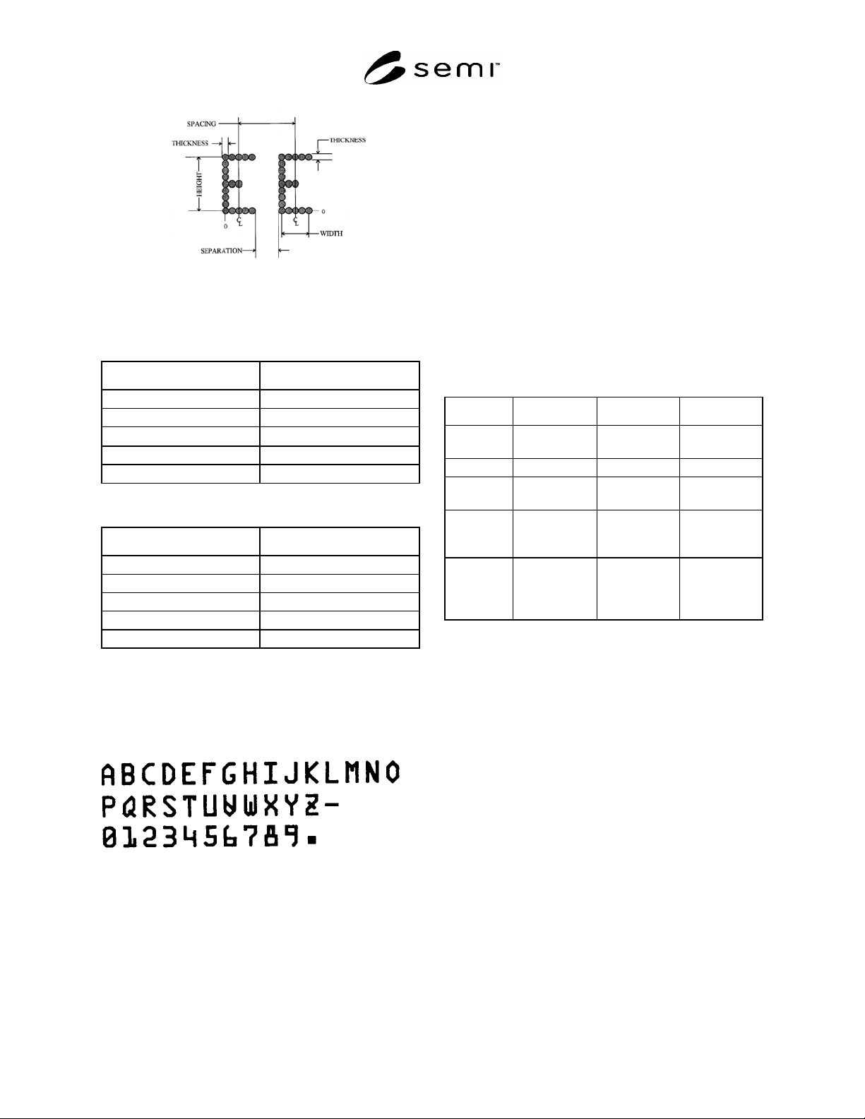
5.1 Dot matrix method shall be used to write charac-
ters. The minimum matrix shall be 5 dots horizontal
and 9 dots vertical as shown in Figure 1. More dots
may be used.
NOTE 2: The 5 × 9 dot matrix shown in Figure 1 is the
minimum number of dots allowed. More dots may be used,
up to and including a solid line. A solid line is not
recommended, since it may increase wafer breakage.
5.2 Character Dimensions and Spacing — See Table
1, Table 2, and Figure 1.
SEMI T5-96 © SEMI 1996, 2004 2
Figure 1
Character Outline
Table 1 Character Dimensions and Spacing —
Configuration A — 3”, 100 mm, 125 mm, 150 mm
Character (mm)
Height 1.624 ± 0.025
Width 0.812 ± 0.025
Thickness
0.200 + 0.050
Spacing 1.420 ± 0.025
Minimum Separation 0.400
Table 2 Configuration B — 2”, Option for 3” Wafers
Character (mm)
Height 0.812 ± 0.025
Width 0.406 ± 0.025
Thickness 0.100 ± 0.050
Spacing 0.710 ± 0.025
Minimum Separation 0.104
NOTE 3: The thickness of the diagonal in the letter “N” is
0.138 ± 0.05 mm for single density dot matrix.
5.3 SEMI OCR Standard Character Set — See Figure
2 and Appendix 1.
Figure 2
Standard Character Set
6 Alphanumeric Code
6.1 Code — Limited to one line of 20 characters
maximum (see Figure 3 and Table 3 for an example
using 15 characters). The first five to ten characters are
an identification number which is unique to the ingot
for a given supplier. This is followed by a dash, which
is followed by three digits which indicate the wafer
number, as numbered starting from the seed end of the
ingot. The next two alpha characters identify the
vendor according to SEMI AUX001. The last optional
characters are specified by the vendor or customer. For
example, these characters could be used to differentiate
specifications, orientation, or doping. The character
string (using a five character ingot as example) is
constructed as follows:
Table 3 Vendor identification code
Character # Character Style Parameter Definition
1 - 5 Alphanumeric Ingot number Supplier-
assigned
6 Alpha dash a spacer
7 - 9 Numeric Wafer number Number of
wafer in ingot
10 - 11 Alpha only Vendor
Identification
Code
See SEMI
AUX001
12 - 15 Alphanumeric Optional:
characters to
identify
specification(s)
Supplier- or
customer-
specified