semi合集-English.pdf - 第7482页
SEMI MF1630-0704 © SEMI 2004 2 3.5 Multip le internal reflections can produ ce a secondary interferogram and baseline oscillations. Changing the sample specime n thickness, the surface preparation, or the reso lution can…

SEMI MF1630-0704 © SEMI 2004 1
SEMI MF1630-0704
TEST METHOD FOR LOW TEMPERATURE FT-IR ANALYSIS OF
SINGLE CRYSTAL SILICON FOR III-V IMPURITIES
This test method was technically approved by the Global Silicon Wafer Committee and is the direct
responsibility of the North American Silicon Wafer Committee. Current edition approved for publication by
the North American Regional Standards Committee on March 14, 2004. Initially available at
www.semi.org
May 2004; to be published July 2004. Original edition published by ASTM International as ASTM F 1630-
95. Last previous edition SEMI MF1630-00.
1 Purpose
1.1 Electronic grade polysilicon producers and users
rely on LTFT-IR spectroscopy to evaluate polysilicon
for quality assurance and research purposes.
1.2 LTFT-IR spectroscopy identifies and quantitates
boron, phosphorus, aluminum, arsenic, indium,
antimony, and gallium.
1.3 LTFT-IR spectroscopy can be applied to FZ, CZ, or
other single crystal silicon (either doped or undoped) up
to the concentration limits given in Section 2.2.
1.4 The measurement of carbon in silicon at low
temperature can be accomplished concurrently in
accordance with SEMI MF1391. The carbon can be
measured at lower concentrations at <15 K than is
possible at room temperature because the two-phonon
band transmission is increased by a factor of two
allowing greater throughput to the detector that results
in an increased signal to noise ratio. Also the carbon
adsorption band narrows from a FWHM of 5 to 6 cm
−1
to a FWHM of 2.5 to 3.0 cm
−1
at these low
temperatures.
2 Scope
2.1 This test method covers the determination of
electrically active boron, phosphorus, arsenic,
aluminum, antimony, and gallium concentration in
single crystal silicon.
2.2 This test method can be used for silicon in which
the impurity/dopant concentrations are between 0.01
ppba and 5.0 ppba for each of the electrically active
elements.
2.3 The concentration for each impurity/dopant can be
obtained by application of Beer’s Law. Calibration
factors are given for each element.
NOTICE: This standard does not purport to address
safety issues, if any, associated with its use. It is the
responsibility of the user of this standard to establish
appropriate safety and health guides and determine the
applicability of regulatory or other limitations prior to
use.
3 Limitations
3.1 The sample specimen must be colder than 15 K for
measurement of electrically active species. If the
sample specimen is mounted on a cold finger, care must
be taken to obtain good contact between the sample
specimen and the cold finger for efficient heat transfer.
The oxygen absorption lines at 1136 cm
−1
and 1128
cm
−1
are sensitive to temperature and can be used to
determine the specimen temperature.
1
When the
sample specimen is less than 15 K the net absorbance at
1136 cm
−1
is three times larger than the net absorbance
at 1128 cm
−1
. A ratio of greater than three is obtained
for temperatures below 15 K.
3.2 Without sufficient incident white light the
compensated donors and acceptors will not absorb.
Therefore, the white light intensity must be great
enough to completely neutralize all the compensated
donors and acceptors. The intensity of the white light
necessary must be determined for each system. The
user should increase the intensity of the white light until
further increase in intensity no longer affects the
area/height of the electrically active impurity/dopant
peaks.
3.3 Water vapor absorption interferes with the
measurement of several peaks. Consequently, the
background spectrum should be collected at least daily.
The entire light path, including the sample chamber,
must be purged to remove moisture. Special care
should be taken whenever a sample specimen is
changed so that the moisture level in the sample
chamber or elsewhere in the light path is not affected.
3.4 Oxygen level in Czochralski silicon can be high
enough to exhibit thermal donor absorption lines.
These lines fall between 400 cm
−1
and 550 cm
−1
and
can interfere with aluminum (473 cm
−1
), gallium (548
cm
−1
), and occasionally arsenic (382 cm
−1
). Thermal
donors can be removed by annealing the sample
specimen.
1 Rome, J. J., “Calibration Relationships for Optically Measuring the
Concentrations of Boron, Gallium and Indium in Silicon,” Thesis,
School of Engineering, Air Force Institute of Technology (1982), pp.
46–47.

SEMI MF1630-0704 © SEMI 2004 2
3.5 Multiple internal reflections can produce a
secondary interferogram and baseline oscillations.
Changing the sample specimen thickness, the surface
preparation, or the resolution can eliminate the
secondary interferogram and the baseline oscillation.
3.6 High antimony levels interfere with the 320 cm
−1
boron absorption line. Antimony' s strongest absorption
line is 293 cm
−1
, but a secondary absorption line occurs
at 320 cm
−1
.
4 Referenced Standards
4.1 SEMI Standards
SEMI MF723 — Practice for Conversion Between
Resistivity and Dopant Density for Boron-Doped,
Phosphorus-Doped, and Arsenic-Doped Silicon
SEMI MF1241 — Terminology of Semiconductor
Technology
SEMI MF1391 — Test Method for Substitutional
Atomic Carbon Content of Silicon by Infrared
Absorption
SEMI MF1723 — Practice for Evaluation of
Polycrystalline Silicon Rods by Float-Zone Crystal
Growth and Spectroscopy
4.2 ASTM Standards
E 131 — Terminology Relating to Molecular
Spectroscopy
2
E 168 Practices for General Techniques of Infrared
Quantitative Analysis
2
E 177 — Practices for Use of the Terms Precision and
Bias in ASTM Test Methods
3
E 275 — Practice for Describing and Measuring the
Performance of Ultraviolet, Visible, and Near-Infrared
Spectrophotometers
2
NOTICE: Unless otherwise indicated, all documents
cited shall be the latest published versions.
5 Terminology
5.1 General definitions for terms related to infrared
absorption spectroscopy are found in ASTM
Terminology E 131.
5.2 Definitions for terms related to silicon materials
technology are found in SEMI MF1241.
2 Annual Book of ASTM Standards, Vol 03.06, ASTM International,
100 Barr Harbor Drive, West Conshohocken, PA 19428. Telephone:
610-832-9500, Fax: 610-832-9555, Website:
www.astm.org
3 Annual Book of ASTM Standards, Vol 14.02.
5.3 Abbreviations and Acronyms
5.3.1 FT-IR — Fourier transform infrared
(spectrometer).
5.3.2 FWHM — full width of an absorption peak
expressed in cm
−1
at half its absorbance magnitude as
measured from the baseline.
5.3.3 LTFT-IR — low temperature, Fourier transform
infrared (spectrometer).
5.4 Definitions
5.4.1 background spectrum, n — in FT-IR instruments,
the single-beam spectrum obtained without a specimen
in the infrared light path that is usually obtained with
only nitrogen, dry air, or a vacuum in the beam.
5.4.2 baseline, n — a straight line interpolation between
points on either side of the absorption peak of the
absorbance spectrum.
5.4.3 electrically active elements, n — dopants or impu-
rities in silicon that are members of either Group III
(boron, aluminum, gallium, and indium) or Group V
(phosphorus, arsenic, antimony, and bismuth) of the
periodic table.
5.4.4 sample spectrum, n — the ratio of a spectrum
obtained with the test specimen in the IR beam to a
background spectrum.
6 Summary of Test Method
6.1 A sample specimen of single crystal silicon is
cooled to less than 15 K. Under these conditions the
number of free carriers becomes negligibly small and
the IR spectrum of the sample exhibits a series of
absorption bands that are characteristic for each shallow
impurity species.
4
6.2 The sample specimen is illuminated with an
incident white light source to flood the silicon with
photons of greater energy than the silicon band gap to
allow neutralization of compensated impurities.
5
6.3 An infrared beam is directed through the sample
specimen and a transmitted spectrum is collected. The
spectrum is ratioed to the background spectrum and
then converted to an absorbance spectrum.
6.4 Baselines are constructed at one of the characteristic
absorption bands for each impurity/dopant to be
measured.
4 Kolbesen, B. O., “Simultaneous Determination of the Total
Content of Boron and Phosphorus in High-Resistivity Silicon by IR
Spectroscopy at Low Temperature,” Appl. Phys . Lett. 27, 353–355
(1975).
5 Baber, S. C., “Net and Total Shallow Impurity Analysis of Silicon
by Low Temperature Fourier Transform Infrared Spectroscopy,” Thin
Solid Films 72, 201–210 (1980).
SEMI MF1630-0704 © SEMI 2004 3
6.5 The areas of the absorption bands are measured.
6.6 Concentrations of each impurity/dopant are
calculated in accordance with Bouguer-Beer’s Law
with factors given in this test method.
7 Apparatus and Materials
7.1 Cryostat — To maintain the sample specimen
temperature below 15 K. This cryostat may be liquid
helium immersion, exchange gas, or closed cycle
refrigeration.
7.2 Sample Specimen Holder — Constructed of high
heat conductivity metal with an aperture(s) to block any
of the infrared beam except that passing through the
sample.
NOTE 1: The procedure of Section 11 is based on the
assumption that the cryostat can accommodate and utilizes a
multi-sample holder.
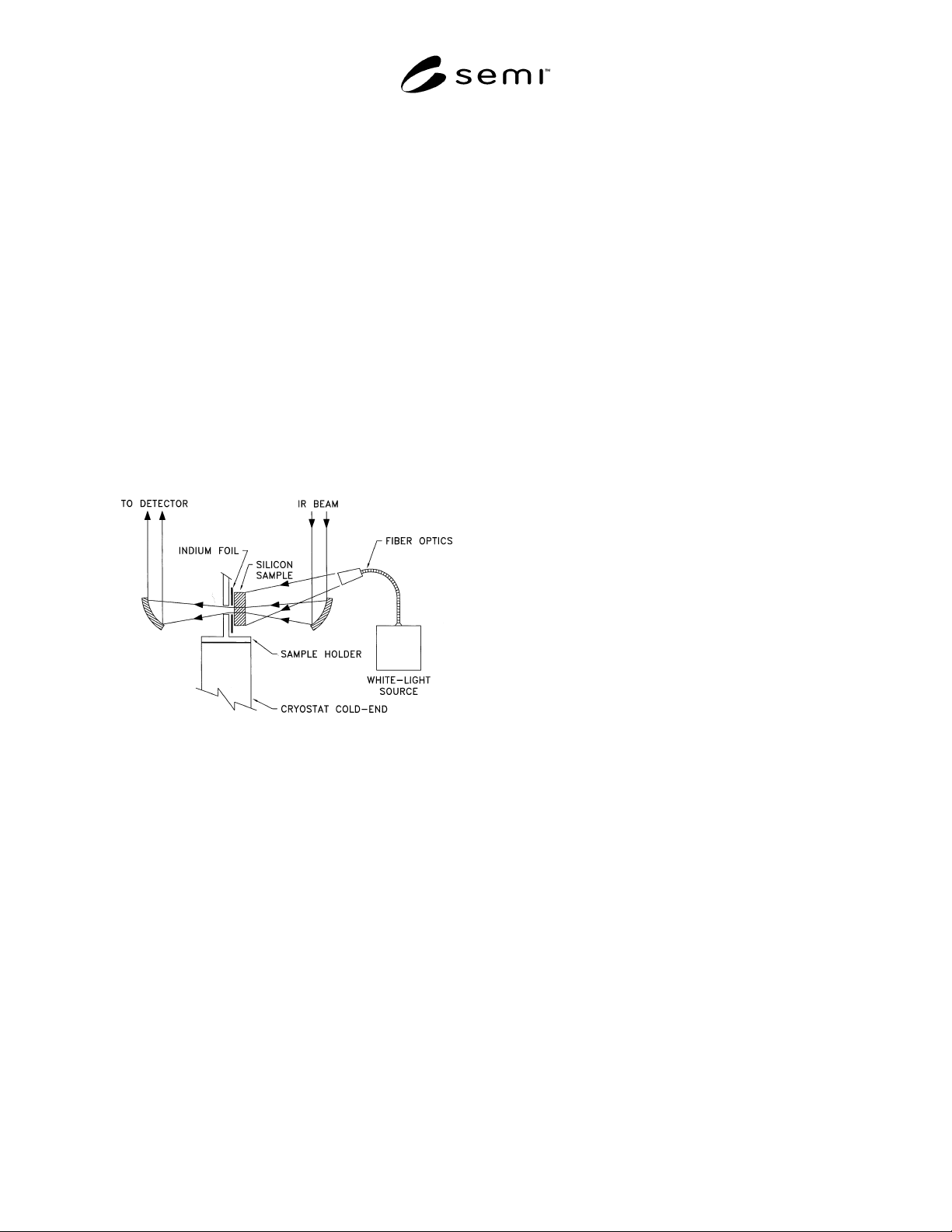
7.3 White-light Source — As shown in Figure 1.
Figure 1
Sample Holder and Optics Suitable for Illumination
with White Light via Fiber Optics
7.4 Fourier Transform Infrared Spectrometer (FT-IR)
— Must be equipped with suitable optics and detector
for use in the region from 250 cm
−1
to 1300 cm
−1
.
7.4.1 The spectrometer shall be capable of at least 1.0
cm
−1
resolution. The resolution shall be sufficient so
that after zero-filling, apodization, and Fourier
transformation the phosphorus adsorption band at 315.9
cm
−1
has a FWHM not to exceed 1.1 cm
−1
.
7.4.2 The detector shall be sufficiently sensitive to
provide a reasonable signal to noise response in the
desired spectral region. A room temperature DTGS
with a CsI window suffices for the higher
concentrations of elements in this test method.
However, a zinc-doped germanium Ge:Zn detector
operated at 4.4 to 10.0 K is preferred to give a signal-
to-noise ratio sufficient to properly determine the
elements at the lower concentrations and for improved
precision.
7.5 Calcium Fluoride Crystal (CaF
2
) — Cut to nominal
thickness of 5 mm.
8 Sample Preparation
8.1 If the samples are from polysilicon, they must first
be converted to single crystal in accordance with SEMI
MF1723 or other established means.
8.2 Sample specimen shall be cut and polished to fit the
sample specimen holder. The surface may be
mechanically or chemically polished. Each sample
specimen shall have a thickness variation of less than
1% of overall thickness.
8.3 For measurement of electrically active impurities,
the sample specimen thickness should be as follows:
8.3.1 For high purity silicon (>2000 Ω·cm): 3 to 5 mm
to allow for lower detection limits.
8.3.2 Between 5 and 20 mm in cases where impurity
levels to be measured are below 0.01 ppba.
8.3.3 For heavily doped silicon (<10 Ω·cm): 1 to 2 mm
to allow greater transmission of the infrared radiation.
9 Reference Specimens
9.1 One or more silicon samples that contain impurities
in the range of the samples to be tested shall be
classified as reference specimens. These reference
specimens should be analyzed repeatedly and
periodically according to this test method. Compare the
results obtained to previous data to establish that the
measurement process is in control.
10 Testing of the Instrument
10.1 Establish FT-IR instrument stability by checking
the 100% transmittance line.
10.1.1 Collect and store two background spectra
sequentially through an open aperture of the cryostat
specimen holder.
10.1.2 Ratio these two spectrum to obtain a
transmittance spectrum.
10.1.3 Examine the spectrum from 1200 cm
−1
to 250
cm
−1
. The spectrum should be 100 ± 0.5% T over this
range. Proceed only if the spectrum is 100 ± 5% over
this range, otherwise correct any instrumental
instability.