semi合集-English.pdf - 第5755页
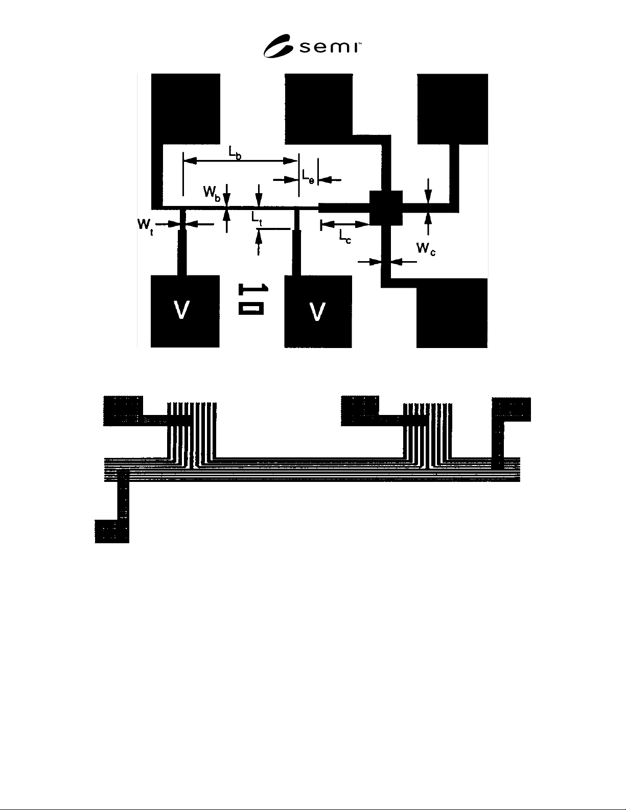
SEMI P19-92 © SEM I 1992, 1996 6 Figure 13 Electrical Cell, 2 × n Configura tion with La beling Figure 14 Blow-Up of Bri dge Resi stor with Proxim ity Lines
SEMI P19-92 © SEMI 1992, 19965
across the ends) is provided on the array to allow
recognition of the cell as a unit.
3.2.7 Electrical Cell — (See Figure 12.)
3.2.7.1 The electrical cell is designed to provide very
precise and relatively fast determinations of the average
linewidth of a conductive film using an automated test
system, but can also be used with a manual prober.
3.2.7.2 The design elements of this cell are the bridge
resistor linewidth, W
b
, the center-of-tap to center-of-tap
bridge length, L
b
, the sheet and bridge tap widths, W
c
and W
t
, the sheet and bridge tap lengths, L
c
and L
t
, the
extension of the bridge resistor line to the nearest
discontinuity in that line, L
e
, and the size of the square
sheet will be 35 – 100 µm. See Figure 13 for the
labeling of these elements. The rules for these elements
are as follows:
W
t
≤ W
b
(for L
b
< 100 W
b
)(1)
W
t
≤ 1.2*W
b
(for L
b
≥ 100 W
b
and W (2)
L
b
≥ 15W
b
for 80 µm, whichever is larger) (3)
L
t
> 2W
t
(4)
L
e
> 2W
b
(5)
L
c
> 2W
c
(6)
3.2.7.3 The cell consists of two types o f four-point
Kelvin structures: a van der Pauw sheet resistor and one
or more bridge resisitors. The orientation of the
individual bridge resistors is user-defined. The bridge
resisitors also can be surrounded by dummy lines to
measure the process bias due to proximity effect. On
structures containing the dummy lines, the
interconnects will hook up to the bridge resistor in a
perpendicular fashion, as shown in Figure 14.
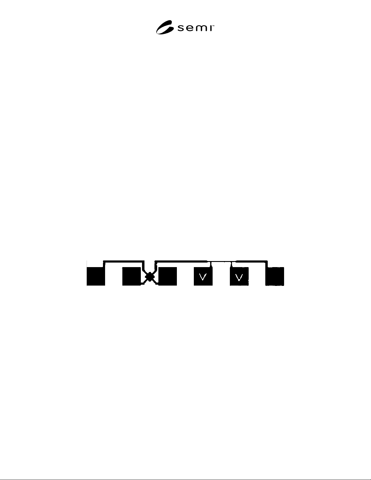
3.2.7.4 The pad labeled with a V in Figures 13 and 15
will be used for voltage measurement only, and will be
used as the fourth point in the sheet resistivity
measurements that will be used to make the linewidth
determination.
SEMI P19-92 © SEMI 1992, 1996 6
Figure 13
Electrical Cell, 2 × n Configuration with Labeling
Figure 14
Blow-Up of Bridge Resistor with Proximity Lines
SEMI P19-92 © SEMI 1992, 19967
3.2.7.5 The pads can be arranged in a 1 × n layout for
scribeline placement (see Figure 15), or the
conventional 2 × n layout can be used if the spatial
constraints are minimal. Pad size and pitch are user-
defined. For automatic testing in a production
environment, it is recommended that the pads be 80 –
100 mm per side.
3.3 User Considerations
3.3.1 Target CD versus Resolved CD
3.3.1.1 The desired size of a critical d imension (CD)
on an integrated circuit can be considered its nominal
value and is herein designated the “target CD.” The size
actually achieved (resolved CD) on the circuit may be
different from this nominal value.
3.3.1.2 Measurements of the resolved CD may not be
accurate because of the difficulty in determining the
actual location of the edge in the optical or SEM image
profile.
3.3.1.3 Even if inaccurate, measurement of the
resolved CD can be valuable for comparison purposes if
the measurement method has adequate precision and
sensitivity to detect the dimensional changes of interest.
3.3.1.4 The traditional definition of re solution may not
be adequate (e.g., ability to distinguish closely spaced
points) for specifying the sensitivity to small
dimensional changes.
4 References
4.1 Yen, D., Linholm, L.W., and Buehler, M.G., “A
Cross-Bridge Test Structure for Evaluating the
Linewidth Uniformity of an Integrated Circuit
Lithography System,” J. Electrochemical Society
1_2_9_ (1982), 2313.
4.2 Hasan, T.F., Perloff, D.S., and Mallory, C.L.,
“Test Structures for the Measurement and Analysis of
VLSI Lithographic and Etching Parameters”,
Semiconductor Silicon/1981, H.R. Huff, R.J. Kriegler
and Y. Takeishi Eds., (Electrochemical Society,
Pennington, NJ) 1981, 866.
4.3 Carver, G.P., Mattis, R.L., and Buehler, M.G.,
“Design Considerations for the Cross-Bridge Sheet
Resistor,” NBSIR 82-2548, National Bureau of
Standards, Washington, DC, (1982).
4.4 Buehler, M.G., Hershey, C.W. , “The Split-Cross-
Bridge Resistor for Measuring the Sheet Resistance,
Linewidth, and Line Spacing of Conducting Layers,”
IEEE Transactions on Electron Devices, (1986), 1572.
4.5 Lin, Burn J., “Proximity and Astigmatism Tolerant
Testsites for Electrical Linewidth Measurement,” SPIE
Proc., Vol. – (1989).
Figure 15
Electrical Cell, 1 × n Configuration