semi合集-English.pdf - 第5770页
SEMI P21-92 © SEMI 1992, 2003 5 Figure 3 NOTICE: SEMI makes no warranties or representatio ns as to the suitability of th e standards set forth herein for any particular application. Th e determination of the suitability…
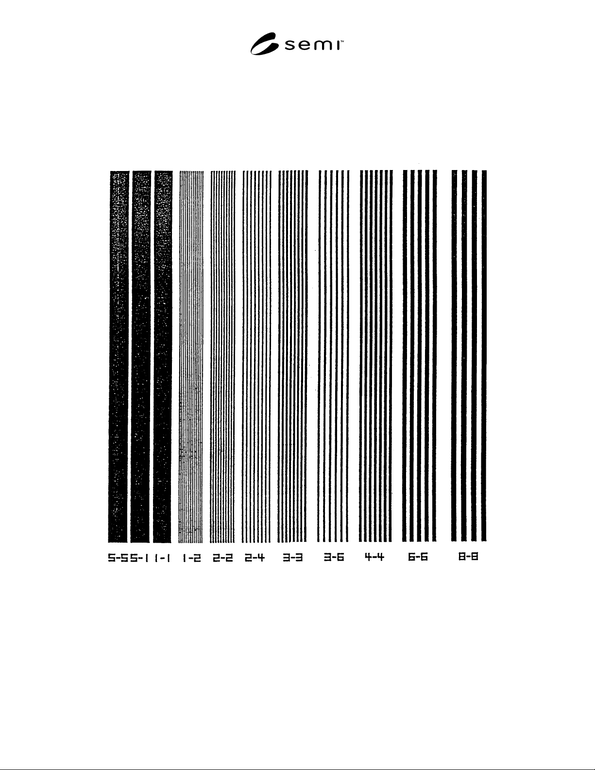
SEMI P21-92 © SEMI 1992, 2003 4
Figure 2
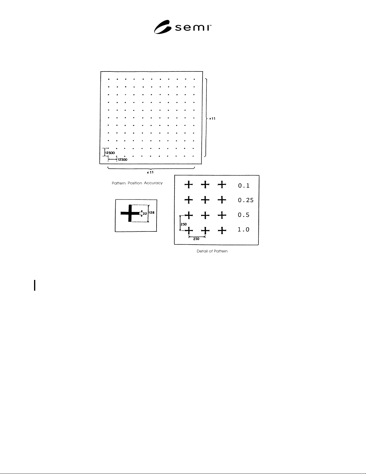
SEMI P21-92 © SEMI 1992, 2003 5
Figure 3
NOTICE: SEMI makes no warranties or representations as to the suitability of the standards set forth herein for any
particular application. The determination of the suitability of the standard is solely the responsibility of the user.
Users are cautioned to refer to manufacturer’s instructions, product labels, product data sheets, and other relevant
literature respecting any materials mentioned herein. These standards are subject to change without notice.
The user’s attention is called to the possibility that compliance with this standard may require use of copyrighted
material or of an invention covered by patent rights. By publication of this standard, SEMI takes no position
respecting the validity of any patent rights or copyrights asserted in connection with any item mentioned in this
standard. Users of this standard are expressly advised that determination of any such patent rights or copyrights, and
the risk of infringement of such rights, are entirely their own responsibility.
Copyright by SEMI® (Semiconductor Equipment and Materials
International), 3081 Zanker Road, San Jose, CA 95134. Reproduction o
f
the contents in whole or in part is forbidden without express written
consent of SEMI.

SEMI P22-0699 © SEMI 1993, 19991
SEMI P22-0699
GUIDELINE FOR PHOTOMASK DEFECT CLASSIFICATION AND SIZE
DEFINITION
This guideline was technically approved by the Global Mask & Mask Equipment Committee and is the direct
responsibility of the Japanese Mask & Mask Equipment Committee. Current edition approved by the
Japanese Regional Standards Committee on March 17, 1999. Initially available at www.semi.org April 1999;
to be published June 1999. Originally published in 1993.
1 Purpose
1.1 The purpose of this guideline is to establish stan-
dard nomenclature for photomask defect classifications,
and to define defect sizing methods.
2 Scope
2.1 It is desirable to follow this guideline when
discussing classification, nomenclature, and size of the
photomask defects.
3 References
3.1 SEMI Standard
SEMI P33 — Provisional Specification For
Developmental 230 mm Square Hard Surface
Photomask Substrates.
4 Terminology
4.1 design pattern — pattern of intended design data.
4.2 photomask pattern — pattern on photomask
surface.
4.3 Many terms relating to photomask technology can
be found in SEMI P33.
5 Classification of the Mask Defect
5.1 Mask Pattern Defects
5.1.1 Shape Defect — a photomask pattern whose
shape is different from its intended design pattern.
5.1.1.1 Isolated Defect — shape defects which are
isolated from pattern.
1) Dot (See Figures 1, 23)
2) Hole (See Figure 2)
5.1.1.2 Edge Defect — shape defects which are
adjacent to straight pattern edge.
1) Edge Extension (See Figures 3, 24)
2) Edge Intrusion (See Figure 4)
5.1.1.3 Corner Defect — shape defects which are
adjacent to corners.
1) Corner Extension (See Figures 5, 27, 29)
2) Corner Intrusion (See Figures 6, 28, 30)
5.1.1.4 Bridge — shape defects which are adjacent to
more than two edges.
1) Opaque Bridge (See Figures 7, 26)
2) Clear Bridge (See Figure 8)
5.1.2 Size Defect — a photomask pattern whose size is
different from its intended design pattern.
1) Oversize (on opaque pattern) (See Figure 9)
2) Oversize (on clear pattern) (See Figure 10)
3) Undersize (on opaque pattern) (See Figure 11)
4) Undersize (on clear pattern) (See Figure 12)
5) Elongation (on opaque pattern) (See Figure 13)
6) Elongation (on clear pattern) (See Figure 14)
7) Truncation (on opaque pattern) (See Figure 15)
8) Truncation (on clear pattern) (See Figure 16)
5.1.3 Misplacement Defect — a photomask pattern
whose placement is different from its intended design.
(See Figures 17, 18, 25)
5.1.4 Transmission Defect — a photomask pattern
whose transmission is different from its intended
design.
1) Transmission Defect (on clear pattern) (See Figure
19)
2) Transmission Defect (on opaque pattern) (See
Figure 20)
5.1.5 Missing pattern defect — a photomask pattern
which is absent.
1) Missing opaque pattern (See Figure 21)
2) Missing clear pattern (See Figure 22)
5.2 Glass Defect — unwanted defect in (or on) a glass
created by various undefined causes (e.g. sleek, pit,
scratch, chip, striation, polishing mark, discolor,
bubbles, etc.).
5.3 Miscellaneous Defect — unwanted clear or opaque
spot created by various undefined causes (e.g., crystal