semi合集-English.pdf - 第5313页
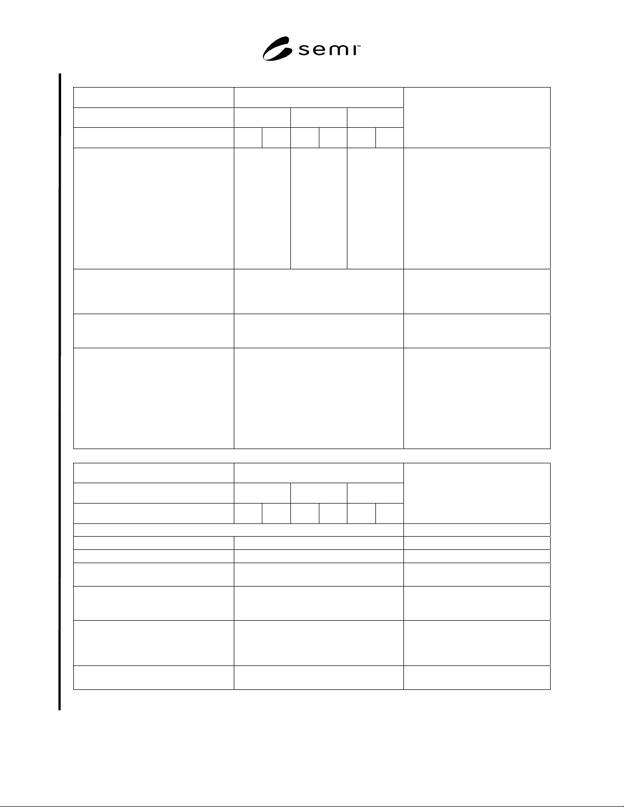
SEMI M49-0704 © SEMI 2001, 2004 12 3. SETUP PARAMETERS Item Recommended Specification Technology Generation 130 nm 90 nm 65 nm Grade A B A B A B Comments and References 3.1 Nominal Edge Exclusion defining FQA (mm) ≥ 2 ≥ …
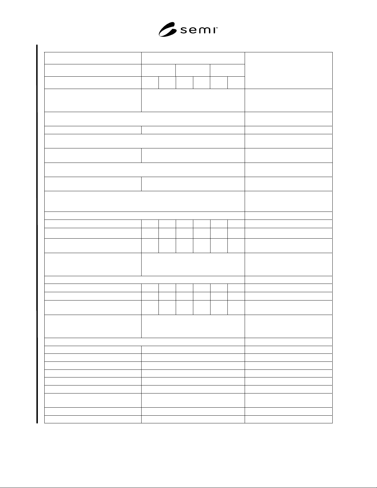
SEMI M49-0704 © SEMI 2001, 2004
11
2. MEASUREMENT FUNCTIONS
Item Recommended Specification
Technology Generation 130 nm 90 nm
9
65 nm
9
Grade A B A B A B
Comments and References
2.1.5.4 Spatial Bandwidth
f
min
(mm
–1
)
f
max
(mm
–1
)
0
1
Nominal value ± 5% tolerance
2.1.6 Other Global Flatness Parameters SEMI M1 Appendix 1; SEMI
MF1530; JEIDA 43; DIN 50441-5
2.1.6.1 GFLR, GFLD required
2.1.7 Other Local Flatness Parameters SEMI M1 Appendix 1; SEMI
MF1530; JEIDA 43; DIN 50441-5
2.1.7.1 SPID, SFLR, SFLD, SFQD,
SFSR, SFSD
required
2.1.8 Other Shape Parameters SEMI M1 Appendix 2; SEMI
MF1390; JEIDA 43; DIN 50441-5
2.1.8.1 Sori (GFLYFER), Bow
(GM3YMCD), Warp (GB3NMPR)
required
2.2 Nanotopography These parameters refer to flatness
measurement of individual surfaces;
see SEMI M43.
2.2.1 Analysis Area Size = 2 mm
2.2.1.1 Level 3 Variability σ
3
(nm, 1 σ) ≤ 0.7 ≤ 1.3 ≤ 0.5 ≤ 1.1 ≤ 0.3 ≤ 0.7
2.2.1.2 Matching Tolerance ∆
m
(nm) ≤ 1
≤
≤ 0.8 ≤ 1.6 ≤ 0.5 ≤ 1
2.2.1.3 Bias (nm)
≤ 1 ≤ 2 ≤ 0.8 ≤ 1.6 ≤ 0.5 ≤ 1
target until certified reference
materials are available
2.2.1.4 Spatial Bandwidth
f
min
(mm
–1
)
f
max
(mm
–1
)
0.05
2.5
Nominal value ± 5% tolerance;
optionally a range of f
min
= 0.25 mm
–1
to f
max
= 2.5 mm
–1
2.2.2 Analysis Area Size = 10 mm
2.2.2.1 Level 3 Variability σ
3
(nm, 1 σ) ≤ 2.5 ≤ 5 ≤ 1.7 ≤ 3.3 ≤ 1.2 ≤ 2.3
2.2.2.2 Matching Tolerance ∆
m
(nm) ≤ 3.8 ≤ 7.5 ≤ 2.5 ≤ 5 ≤ 1.8 ≤ 3.5
2.2.2.3 Bias (nm)
≤ 3.8 ≤ 7.5 ≤ 2.5 ≤ 5 ≤ 1.8 ≤ 3.5
target until certified reference
materials are available
2.2.2.4 Spatial Bandwidth
f
min
(mm
–1
)
f
max
(mm
–1
)
0.05
2.5
Nominal value ± 5% tolerance;
optionally a range of f
min
= 0.05 mm
–1
to f
max
= 0.5 mm
–1
2.3 Other Parameters
2.3.1 Waviness user specific
2.3.2 Height (individual wafer surfaces) user specific
2.3.3 Slope user specific
2.3.4 Curvature user specific
2.3.5 Line Scans user specific
2.3.6 Contour Maps user specific
2.3.7 Data Histogram 10 or more bins per channel, arbitrarily
definable, cumulative differential
2.3.8 Edge Roll-off user specific
2.3.9 Additional Parameters user specific
SEMI M49-0704 © SEMI 2001, 2004 12
3. SETUP PARAMETERS
Item Recommended Specification
Technology Generation 130 nm 90 nm 65 nm
Grade A B A B A B
Comments and References
3.1 Nominal Edge Exclusion defining
FQA (mm)
≥ 2
≥
≥ 1
Performance parameters are to be
verified with nominal edge exclusion
≥ 2 mm. Instrument must be capable
of reporting to nominal edge
exclusion ≥ 1 mm. As a guide, the
extended performance for nominal
edge exclusion < 2 mm should not
exceed the performance (σ
3
,
matching, bias) by more than 100 %
as compared to ≥2 mm edge exclusion
given appropriate reference material.
3.2 Site Patterns For local flatness: use any site pattern
compatible with SEMI M1; for
nanotopography use floating sites
Recommended range for site size: 5 –
40 mm, arbitrary combination of
length of rectangular sides; see SEMI
M1, SEMI M43
3.3 Sorting Criteria Sorting is performed by using logical
“AND/OR” combinations of multiple
parameters
3.4 Exclusion Windows a) > 3, curved or linear boundaries with
arbitrary position anywhere on the
entire wafer surface
b) perimeter exclusion windows: N zones
with total area covered ≤ 0.001 of total
wafer area in the range R – 2 mm to R,
total perimeter excluded at R – 1 mm
≤ 4% of total wafer circumference, no
single zone longer than 5 mm.
a) e.g., laser mark exclusion
4. PERFORMANCE
Item Recommended Specification
Technology Generation 130 nm 90 nm 65 nm
Grade A B A B A B
Comments and References
4.1 Throughput
4.1.1 200 mm Wafers > 60 wafers per hour
4.1.2 300 mm Wafers > 40 wafers per hour
4.2 Downward Compatibility At least one previous tool generation of
supplier
Specific tools involved need to be
identified
4.3 Calibration Automated method, Certified Reference
Material (CRM) to be provided by
equipment supplier.
4.3.1 Level 3 Variability Test Interval
≥ 10 measurements over a period of not less
than 2 weeks (See NOTE 1.)
To be performed with throughput
mode used for qualifying product
wafers, 95% confidence interval has
to be less than the specified σ
3
4.4 Dependence of Results on Wafer
Orientation
< 1 σ
3
NOTE 1: This recommended specification is not intended to be a requirement for a two week pre-shipment test. Performance could be verified
through routine SPC (Statistical Process Control).
SEMI M49-0704 © SEMI 2001, 2004
13
APPENDIX 1
SCALING MODELS
NOTICE: The material in this appendix is an official part of SEMI M49 and was approved by full letter ballot procedures on
May 14, 2004.
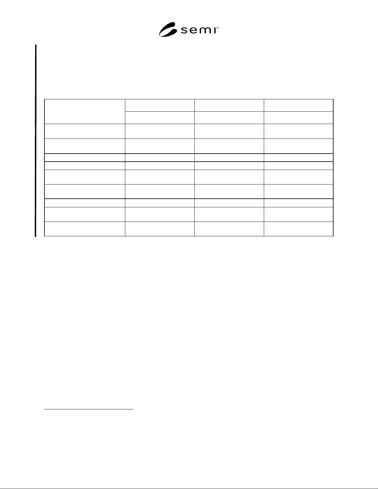
Table A1-1 Scaling models used in Tab. 3.1 for the technology nodes 130 to 65 nm
130 nm node 90 nm node 65 nm node
Property
nominal nominal nominal
1.1 Thickness (200 mm wafers),
µm
725 no scaling no scaling
1.2 Thickness (300 mm wafers),
µm
775 no scaling no scaling
1.3 GBIR, nm 1000 no scaling no scaling
1.4 Site Size local flatness, mm
2
25*25 26*8 26*8
1.4.1 SBIR, including
partial sites, nm
250
2/3 of (120 nm + max. SFQR
per ITRS)
10
2/3 of (120 nm + max. SFQR
per ITRS)
10
1.4.2 SFQR, including
partial sites, nm
130
2/3 of max value acc. to
ITRS
11
2/3 of max value acc. to
ITRS
11
1.5 Warp, µm
30 no scaling no scaling
1.6 Nanotopography, 2 mm, P-V,
nm, at 0.05% defective area
20
2/3 of max value acc. to
ITRS
11
2/3 of max value acc. to
ITRS
11
1.7 Nanotopography, 10 mm, P-V,
nm, at 0.05% defective area
70 70% of previous generation
12
70% of previous generation
12
NOTICE: SEMI makes no warranties or representations as to the suitability of the standards set forth herein for
any particular application. The determination of the suitability of the standard is solely the responsibility of the user.
Users are cautioned to refer to manufacturer’s instructions, product labels, product data sheets, and other relevant
literature respecting any materials mentioned herein. These standards are subject to change without notice.
The user’s attention is called to the possibility that compliance with this standard may require use of copyrighted
material or of an invention covered by patent rights. By publication of this standard, SEMI takes no position
respecting the validity of any patent rights or copyrights asserted in connection with any item mentioned in this
standard. Users of this standard are expressly advised that determination of any such patent rights or copyrights, and
the risk of infringement of such rights, are entirely their own responsibility.
10 120 nm is calculated to be the average taper contribution to SBIR for 130 nm node (SBIR – SFQR). This value is kept constant for the 90 and
65 nm technology nodes.
11 ITRS provides maximum specifications regarding starting material requirements. This maximum value is assumed to be equivalent to the
upper end of range recommended for reference wafers as defined in 6.5.17. The nominal value is then 2/3 of the maximum value.
12 ITRS provides no guidance regarding Nanotopography of 10 mm analysis area
Copyright by SEMI® (Semiconductor Equipment and Materials
International), 3081 Zanker Road, San Jose, CA 95134. Reproduction o
f
the contents in whole or in part is forbidden without express written
consent of SEMI.