semi合集-English.pdf - 第180页
SEMI E22.1-1296 © SEMI 1992, 2002 1 SEMI E22.1-1296 (Reapproved 1102) CLUSTER TOOL MODULE IN TERFACE 300 mm: TRANSPORT MODULE END EFFECTOR EX CLUSION VOLUME STANDARD This standard was technically rea pproved by the Globa…
SEMI E22-0697 © SEMI 1991, 2002 6
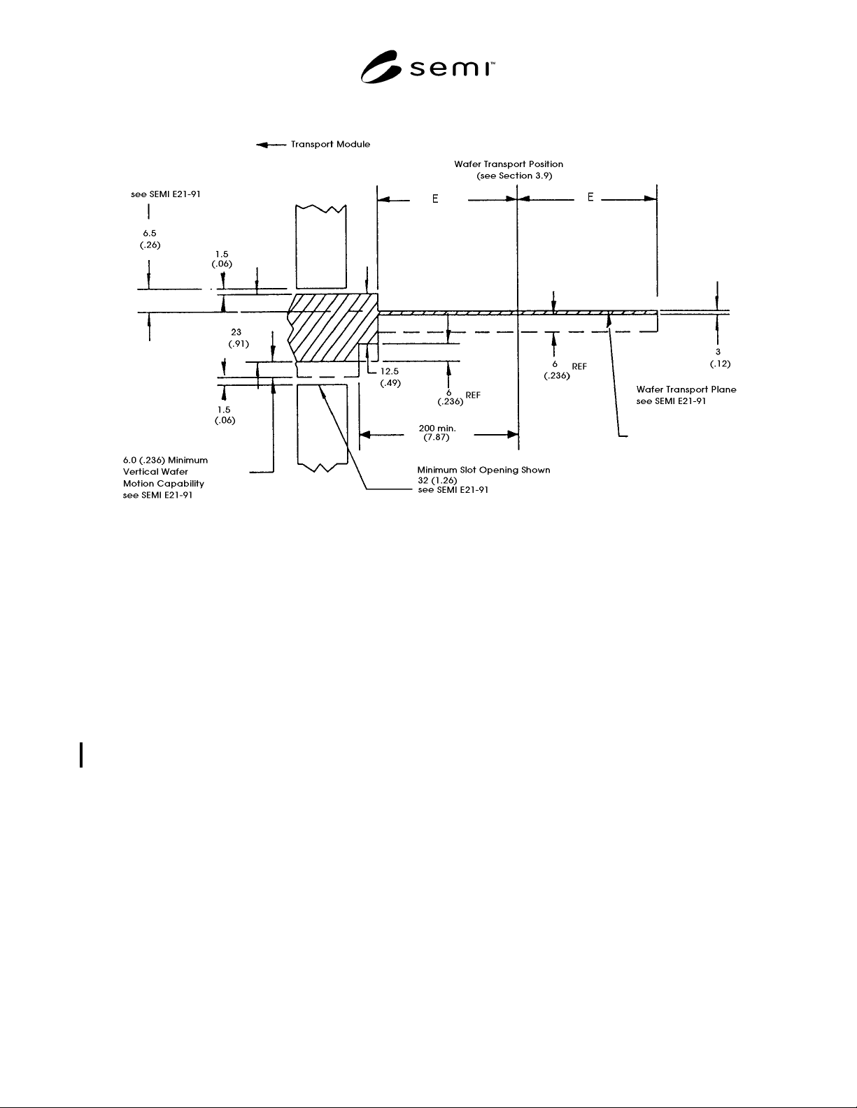
Figure R1-1
Vertical Plane Exclusion Zone (Elevation View)
(Restricted Case for SEMI Standard Cassette Access)
NOTICE: The user’s attention is called to the possibility that compliance with this standard may require use of an
invention covered by patent rights. By publication of this standard, Semiconductor Equipment and Materials
International (SEMI) takes no position respecting the validity of any patent rights asserted in connection with any
item mentioned in this standard. In particular, users of the specification should be aware that Drytek, Inc., A Unit of
General Signal, 16 Jonspin Road, Wilmington, MA 01887-1087, Phone: (508) 657-3933, has neither claimed nor
disclaimed that compliance with this specification would require use of an invention covered by one or more of its
patents. Users of this standard are expressly advised that determination of any such patent rights, and the risk of the
infringement of such rights, are entirely their own responsibility.
NOTICE: SEMI makes no warranties or representations as to the suitability of the standards set forth herein for any
particular application. The determination of the suitability of the standard is solely the responsibility of the user.
Users are cautioned to refer to manufacturer' s instructions, product labels, product data sheets, and other relevant
literature, respecting any materials or equipment mentioned herein. These standards are subject to change without
notice.
By publication of this standard, Semiconductor Equipment and Materials International (SEMI) takes no position
respecting the validity of any patent rights or copyrights asserted in connection with any items mentioned in this
standard. Users of this standard are expressly advised that determination of any such patent rights or copyrights, and
the risk of infringement of such rights are entirely their own responsibility.
Copyright by SEMI® (Semiconductor Equipment and Materials
International), 3081 Zanker Road, San Jose, CA 95134. Reproduction o
f
the contents in whole or in part is forbidden without express written
consent of SEMI.
SEMI E22.1-1296 © SEMI 1992, 2002 1
SEMI E22.1-1296 (Reapproved 1102)
CLUSTER TOOL MODULE INTERFACE 300 mm: TRANSPORT
MODULE END EFFECTOR EXCLUSION VOLUME STANDARD
This standard was technically reapproved by the Global Physical Interfaces & Carriers Committee and is the
direct responsibility of the North American Physical Interfaces & Carriers Committee. Current edition
reapproved by the North American Regional Standards Committee on July 21, 2002. Initially available at
www.semi.org October 2002; to be published November 2002. Originally published in 1992; previously
published December 1996.
1 Introduction
1.1 The standard provides the requirements to change
the limits of applicability of SEMI E22 from 100 mm to
200 mm diameter wafers to 300 mm diameter wafers.
2 Referenced Standards
2.1 SEMI Standards
SEMI E1.9 — Mechanical Specification for Cassettes
Used to Transport and Store 300 mm Wafers
SEMI E22 — Cluster Tool Module Interface: Transport
Module End Effector Exclusion Volume Standard
3 Requirements
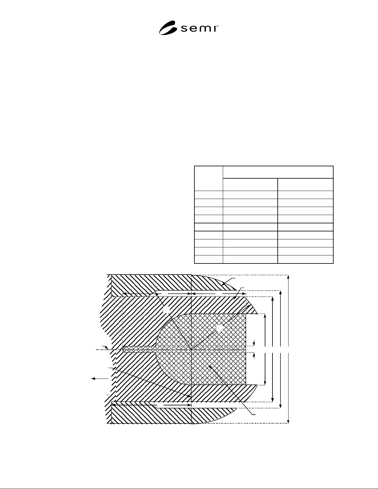
3.1 Wafer Transport Plane Exclusion Zone — All
fixed dimensions remain the same as for SEMI E22
with the following exception. The 25 mm and 10 mm
dimenions for the rectangular space excluded from the
front of the Paddle Exclusion Zone are expanded and
defined by Variables I and H respectively. These
variables are shown in Figure 1. Variables for 250 mm
and 300 mm diameter wafers are specified in Table 1.
Table 1 Wafer Transport Plane Exclusion Zone
Dimensions for 250 mm and 300 mm Diameter
Wafers
Wafer Size
Vbl
250 mm (10 in. nom.) 300 mm (12 in. nom.)
A 270 mm (10.63 in.) 320 mm (12.60 in.)
B 215 mm (8.46 in.) 250 mm (9.84 in.)
C 130 mm (5.12 in.) 225 mm (8.86 in.)
D 122 mm (4.80 in.) 147 mm (5.79 in.)
E 135 mm (5.31 in.) 160 mm (6.30 in.)
F 145 mm (5.71 in.) 170 mm (6.69 in.)
G 122 mm (4.80 in.) 147 mm (5.79 in.)
H 75 mm (2.95 in.) 154 mm (6.06 in.)
I 117 mm (4.61 in.)
F
G I
Wafer
Transport
Position
Wafer
Transport
A
xis
Fork Exclusion Zone
Paddle Exclusion Zone
Pedestal or Pin
Exclusion Zone
C
H
B
A
Transport
Module
D
E
10 (0.39)
Figure 1
New Wafer Transport Plane Exclusion Zone Dimensions
SEMI E22.1-1296 © SEMI 1992, 2002 2
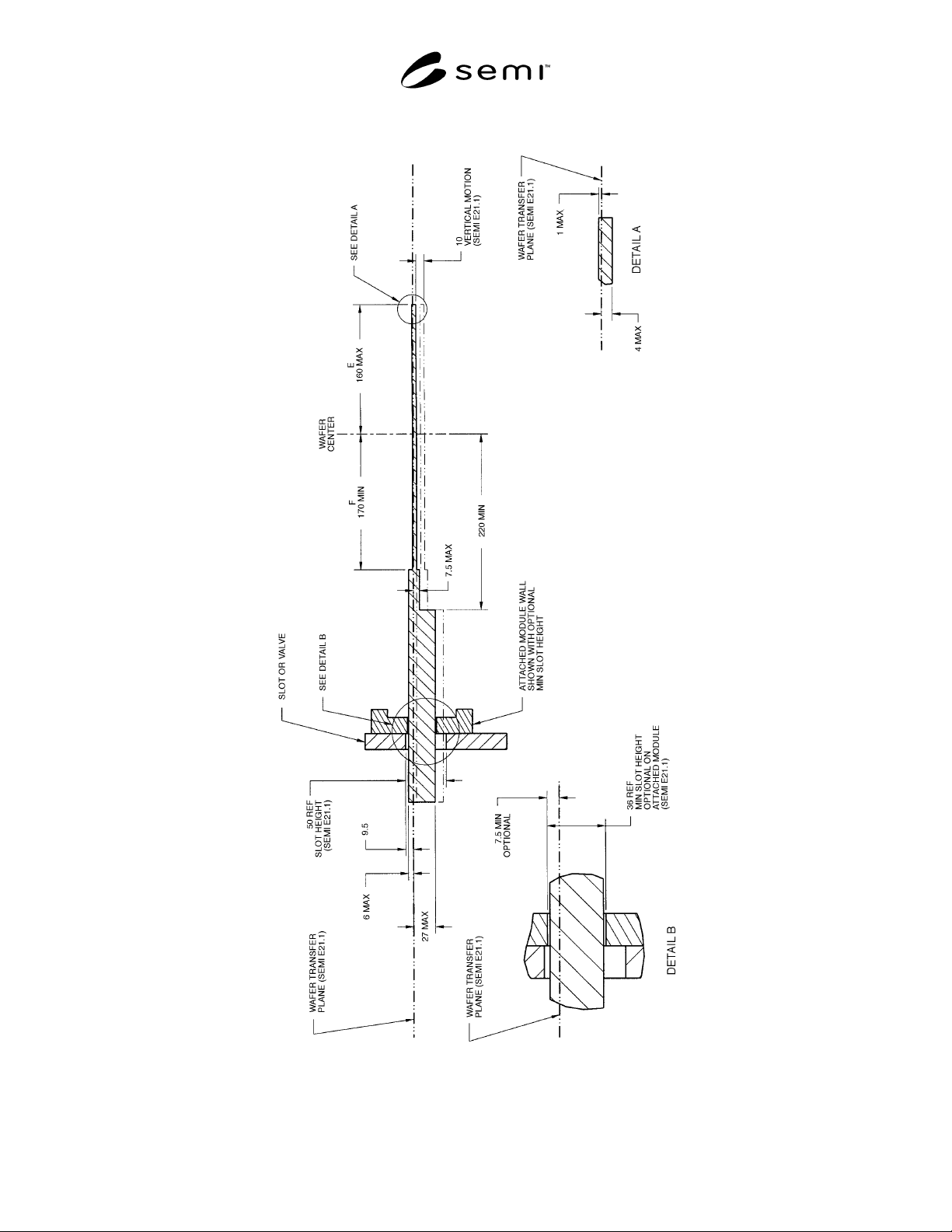
3.2 Vertical Plane Exclusion Zone — This zone is illustrated in Figure 2, which defines dimensional values.
Figure 2
Proposed 300 mm Vertical Plane Exclusion Zone (Elevation View)