semi合集-English.pdf - 第5203页
SEMI M38-1104 © SEMI 1999, 2004 2 NOTICE: Unless otherwise indi cated, all documents cited shall be the latest published versions. 4 Terminology 4.1 Definitions of terms related to silicon wafer technology are gi ven in …

SEMI M38-1104 © SEMI 1999, 2004 1
SEMI M38-1104
SPECIFICATION FOR POLISHED RECLAIMED SILICON WAFERS
This specification was technically approved by the Global Silicon Wafer Committee and is the direct
responsibility of the North American Silicon Wafer Committee. Current edition approved by the North
American Regional Standards Committee on August 16, 2004. Initially available at www.semi.org
September 2004; to be published November 2004. Originally published September 1999; previously
published November 2001.
NOTICE: This document was completely rewritten in
2004.
1 Purpose
1.1 Silicon wafers are often subjected to reclaim
processes in order to improve manufacturing efficiency
in device production. A reclaimed wafer is one that has
been re-conditioned for subsequent utilization.
1.2 This specification covers requirements for
reclaimed silicon wafers to be used for testing and
process monitoring in semiconductor manufacturing.
1.3 In some instances for 300 mm wafers with supplier
marked back surfaces, it is necessary to re-inscribe the
mark after one or more reclaim cycles. Consequently,
this specification also includes an appendix that covers
the re-inscription of such wafers.
NOTE 1: Issues related to the re-inscription of such 300 mm
wafers are discussed in Related Information 1.
2 Scope
2.1 This specification divides reclaimed wafers into
four application categories: Mechanical, Furnace,
Particle, and Lithography and provides tables of the
specification requirements for each category. Thus, a
prospective purchaser of reclaimed silicon wafers needs
to know which application matches his or her
requirements.
2.2 Only requirements for some attributes are specified
in Tables 1 and 2. Other requirements are indicated to
be “customer specified” which means that the customer
may specify a requirement for that particular attribute,
“as-supplied” which means that the attribute has
whatever value was supplied in the wafer delivered (or
used) for reclaim, and “unspecified” which means that
the attribute is not specified and for which the wafer
does not need to be tested.
2.3 In addition to the general categories listed in
Section 2.1, this specification provides requirements for
reclaimed wafers intended for use in advanced device
production, including devices in the 180 and 130 nm
technology generations in a third table.
2.4 This specification is directed specifically to silicon
wafers with one or both polished surfaces. If the wafers
have epitaxial deposits, the attributes of the epitaxial
layer are not included the specification requirements.
2.5 This specification covers reclaim wafers that are
either customer-supplied or third party-sourced. The
user should exercise caution when sourcing materials
with unknown thermal histories, unknown bulk
contamination, or unknown deposits, such as gold (Au)
films.
2.6 For applications placing higher demands on silicon
wafers such as particle counting, measuring pattern
resolution in a photolithography process, or surface ion
contamination monitoring, the customer may want to
reference SEMI M1, SEMI M8, or SEMI M24.
2.7 For referee purposes, U.S. customary units shall be
used for wafers of 2- and 3-inch nominal diameter and
SI (System International), commonly called metric,
units for 100 mm and larger diameter wafers.
NOTICE: This standard does not purport to address
safety issues, if any, associated with its use. It is the
responsibility of the users of this standard to establish
appropriate safety and health practices and determine
the applicability of regulatory or other limitations prior
to use.
3 Referenced Standards
3.1 SEMI Standards
SEMI M1 — Specifications for Polished
Monocrystalline Silicon Wafers
SEMI M8 — Specification for Polished
Monocrystalline Silicon Test Wafers
SEMI M18 — Format for Silicon Wafer Specification
Form for Order Entry
SEMI M24 — Specification for Polished
Monocrystalline Silicon Premium Wafers
SEMI M31 — Provisional Mechanical Specification for
Front Opening Shipping Box Used to Transport and
Ship 300 mm Wafers
SEMI M45 — Provisional Shipping System for 300
mm Wafer Shipping System
SEMI MF1241 — Terminology of Silicon Technology

SEMI M38-1104 © SEMI 1999, 2004 2
NOTICE: Unless otherwise indicated, all documents
cited shall be the latest published versions.
4 Terminology
4.1 Definitions of terms related to silicon wafer
technology are given in SEMI M1 and in SEMI
MF1241.
4.2 The following definitions apply in the context of
this specification:
4.2.1 furnace wafer — a silicon wafer suitable for
monitoring thermal processes or as an implant monitor,
usually used only in a cleanroom environment.
4.2.2 lithography wafer — a silicon wafer used
specifically for testing lithography equipment wherein
surface flatness is the key attribute, usually used only in
a cleanroom environment.
4.2.3 mechanical wafer — a silicon wafer suitable for
equipment or process testing, usually outside of a
cleanroom environment.
4.2.4 particle wafer — a silicon wafer suitable for
monitoring area or process cleanliness, used only in a
cleanroom environment.
4.2.5 reclaimed wafer — a silicon wafer that has been
reconditioned for subsequent utilization.
5 Ordering Information
5.1 Purchase orders for reclaimed silicon wafers
furnished to this specification shall minimally include
the following items:
5.1.1 Nominal diameter,
5.1.2 Type of application (mechanical, furnace,
particle, lithography, 180 nm, or 130 nm),
5.1.3 A statement that the wafers are customer-
supplied or third-party sourced,
5.1.4 Resistivity,
5.1.5 Any other requirement specified by the customer
(indicated as “customer specified” in the tables),
5.1.6 Any requirements that differ from the tables, and
5.1.7 Methods of testing specified attributes for which
either no or multiple test methods exist (see Sections
7.2 and 7.3.
5.2 Customer specified requirements other than
resistivity may include:
5.2.1 Nominal edge exclusion for FQA,
5.2.2 Wafer ID marking,
5.2.2.1 For 300 mm wafers, whether the wafers are to
be re-inscribed as specified in Appendix 1 or not,
5.2.3 Pits, haze, and/or back surface roughness
(particle or lithography wafers),
5.2.4
Localized light scatterers, and
5.2.5 Edge condition (for 200 and 300 mm wafers
only),
5.3 In addition the following optional criteria may be
included in a purchase order:
5.3.1 Minimum removal requirements (if any),
5.3.2 Lot traceability and lot integrity maintenance
requirements,
5.3.3 Lot acceptance criteria,
5.3.4 Certification, and
5.3.5 Packing and Marking.
5.3.5.1 Note that for packing and marking of 300 mm
wafers, the requirements of SEMI M31 and SEMI M45
shall be observed.
6 Requirements
6.1 The wafers shall conform to the parameters as
specified in the appropriate column of Table 1, Table 2,
or Table 3, as augmented and amended by the purchase
order.
6.2 The wafers shall be capable of being reconditioned
for use.
7 Test Methods
7.1 Values of attributes specified in the tables or
purchase order shall be tested in accordance with the
test methods indicated for the attribute in SEMI M1 or
SEMI M18. Sampling for the test shall be done in
accordance with the requirements of SEMI M1.
7.2 If multiple tests are described for any attribute, the
purchase order shall indicate which test shall be used,
unless the supplier of the reclaimed wafers can make
the choice.
7.3 If no standardized test is available for any attribute,
the test method to be used shall be agreed upon between
purchaser and supplier.
8 Certification
8.1 Upon request of the purchaser in the contract or
order, a manufacturer’s or supplier’s certification that
the material was manufactured and tested in accordance
with this specification, together with a report of the test
results, shall be furnished at the time of shipment.
SEMI M38-1104 © SEMI 1999, 2004 3
8.2 In the interest of controlling inspection costs, the
supplier and the purchaser may agree that the material
shall be certified as “capable of meeting” certain
requirements. In this context, “capable of meeting”
shall signify that the supplier is not required to perform
the appropriate tests in Section 9. However, if the
purchaser performs the test and the material fails to
meet the requirement, the material may be subject to
rejection.
9 Packing and Marking
9.1 Special packing requirements shall be subject to
agreement between the supplier and the purchaser.
Otherwise all wafers shall be handled, inspected, and
packed in such a manner as to avoid chipping,
scratches, and contamination, and in accordance with
the best industry practices, to provide ample protection
against damage during shipment.
9.2 The wafers supplied under this specification shall
be identified by appropriately labeling the outside of
each box or other container and each subdivision
thereof in which it may reasonably be expected that the
wafers will be stored prior to further processing.
9.3 For 300 mm wafers, the packing and marking
requirements of SEMI M31 and SEMI M45 shall be
met.
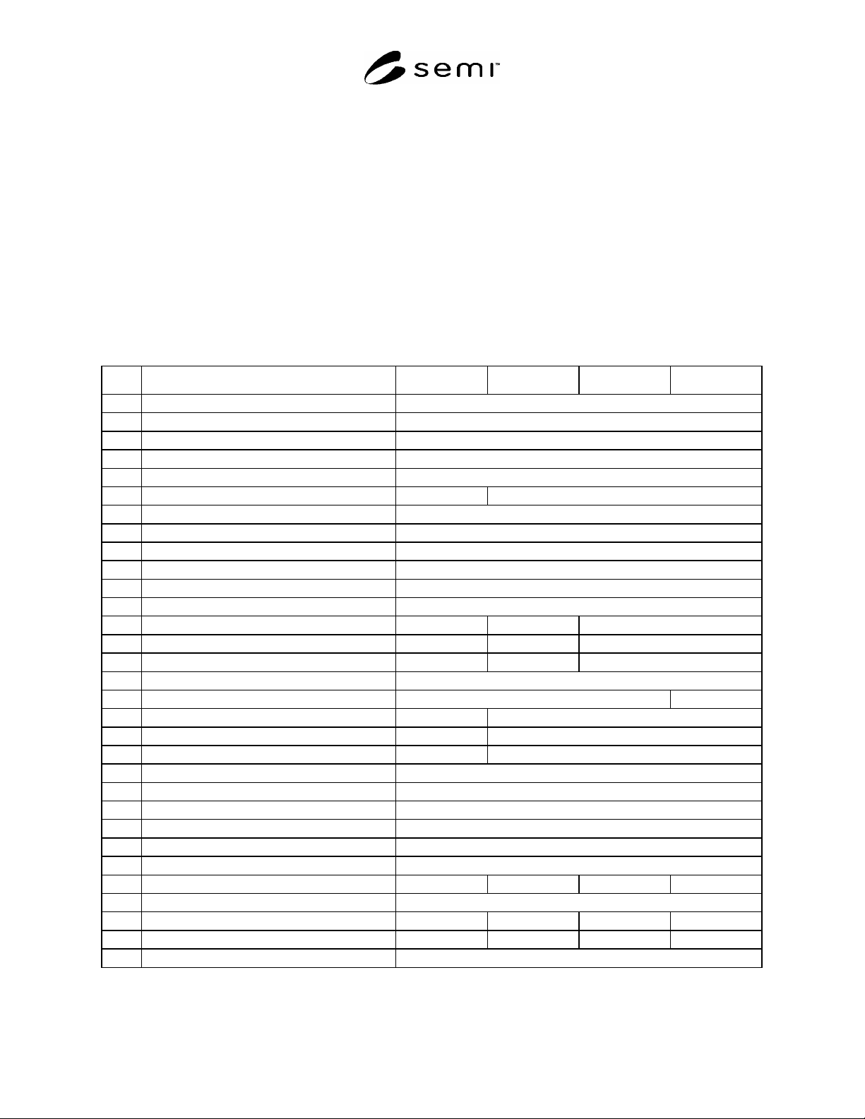
Table 1 Specifications for 150 mm, 200 mm, and 300 mm Silicon Reclaim Wafers
Item Mechanical Furnace Particle Lithography
1.0
General Characteristics
1.1 Growth Method As-supplied
1.2 Crystal Orientation As-supplied
1.3 Conductivity Type As-supplied
1.4 Dopant As-supplied
1.5 Nominal Edge Exclusion for FQA Unspecified Customer specified
2.0
Electrical Characteristics
2.1 Resistivity Customer specified
2.2 Radial Resistivity Variation (RRG) Unspecified
2.3 Resistivity Striations Unspecified
2.4 Minority Carrier Lifetime Unspecified
3.0
Chemical Characteristics
3.1 Oxygen Concentration Unspecified As-supplied Unspecified
3.2 Radial Oxygen Variation Unspecified As-supplied Unspecified
3.3 Carbon Concentration Unspecified As-supplied Unspecified
4.0
Structural Characteristics
4.1 Dislocation Etch Pit Density Unspecified None
4.2 Slip Unspecified None
4.3 Lineage Unspecified None
4.4 Twins Unspecified None
4.5 Swirl Unspecified
4.6 Shallow Pits Unspecified
4.7 OISF Unspecified
4.8 Oxide Precipitates Unspecified
5.0
Wafer Preparation Characteristics
5.1 Wafer ID Marking Customer specified
5.2 Front Surface Thin Films Unspecified None Unspecified None
5.3 Denuded Zone Unspecified
5.4 Extrinsic Gettering Unspecified None Unspecified None
5.5 Backseal Unspecified None Unspecified None
5.6 Annealing Unspecified