semi合集-English.pdf - 第5969页
SEMI P42-0304 © SEMI 2004 2 NOTICE: Unless otherwise indi cated, all documents cited shall be the latest published versions. 5 Terminology 5.1 Definitions 5.1.1 alignme nt mark design — the information related to wafer a…

SEMI P42-0304 © SEMI 2004 1
SEMI P42-0304
SPECIFICATION OF RETICLE DATA FOR AUTOMATIC RECIPE
TRANSFER TO WAFER EXPOSURE SYSTEM
This specification was technically approved by the Global Micropatterning Committee and is the direct
responsibility of the Japanese Micropatterning Committee. Current edition approved by the Japanese
Regional Standards Committee on January 9, 2004. Initially available at www.semi.org February 2004; to be
published March 2004.
1 Purpose
1.1 This specification defines a common data interface,
which consists of frame information of reticle data, in
order to prepare recipes for wafer exposure tools. By
utilizing this interface, it becomes possible to carry out
data handling between design and wafer manufacture so
that the data can be reused during recipe making of
wafer exposure tools. This standard is intended to
assist automatic recipe generation of wafer exposure
tools.
2 Scope
2.1 This standard details frame information in
automatic recipe preparation for wafer exposure
equipment. This standard focuses on communication
interface in work flow of design, mask manufacturing,
and wafer manufacturing processes.
2.1.1 This standard defines the items of the required
and common design information at a reticle design and
a recipe preparation for wafer exposure equipment.
2.1.2 This standard defines a data interface, which can
be commonly used independently to the suppliers and
models of exposure equipment.
NOTICE: This standard does not purport to address
safety issues, if any, associated with its use. It is the
responsibility of the users of this standard to establish
appropriate safety and health practices and determine
the applicability of regulatory or other limitations prior
to use.
3 Limitations
3.1 This data interface is expandable (an item addition
and a user definition are enabled) instead of fixed, and
serves as a form with flexibility.
3.2 This standard uses the current XML standard to
describe a reticle data interface.
3.3 This standard does not provide the definition of the
handling interface of device design data. Only the data
interface specific to frame data information is defined.
3.4 The wafer map information by reticle frame data
and the wafer, which exposure equipment uses, are
defined in this standard.
3.5 This standard includes the handling items of the
related information for reticle exposure and a mark
formation process (reticle) required for automatic recipe
preparation.
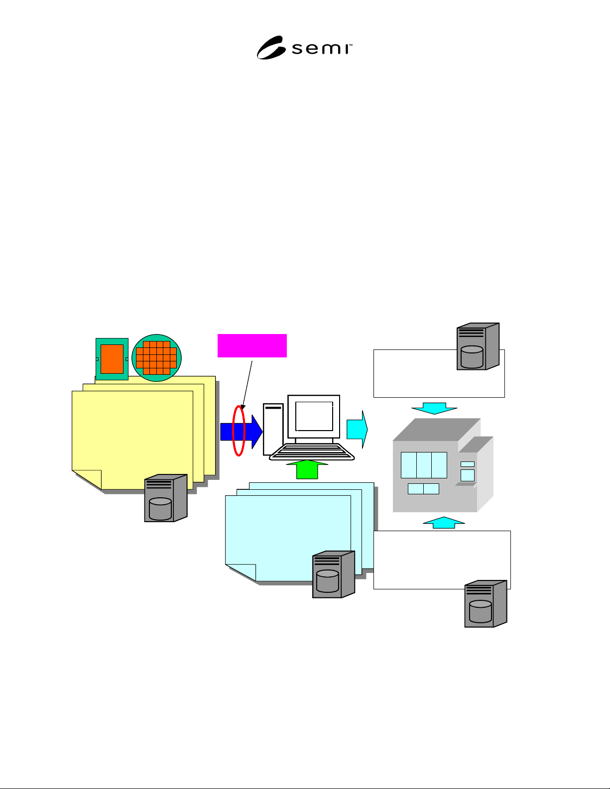
3.6 Recipe preparation is shown in Figure 1. This
document focuses on reticle data management (RDM)
interface (IF) as indicated in Figure 1.
4 Referenced Standards
4.1 JEITA Documents
1
Reticle Data Management Guideline Ver.1.0 (2001) —
(http://jeita-smtc.elisasp.net/)
4.2 World Wide Web Consortium Documents
2
Extensible Markup Language (XML) 1.0 (Second
Edition) — W3C,6 October 2000
(
http://www.w3.org/TR/2000/REC-xml-20001006)
Extensible Markup Language (XML) 1.1 — W3C,15
October 2002 (
http://www.w3.org/TR/2002/CR-xml11-
20021015)
Extensible Markup Language (XML) 1.1 ― 15 October
2002, John Cowan (
http://www.w3.org/TR/2002/CR-
xml-names11-20021218/)
Namespaces in XML — W3C, 14 January 1999
(
http://www.w3.org/TR/1999/REC-xml-names-
19990114/)
XML Schema Part 0: Primer — W3C, 2 May 2001
(
http://www/w3/org/TR/xmlschema-0/)
XML Schema Part 1: Structures — W3C, 2 May 2001
(
http://www/w3/org/TR/xmlschema-1/)
XML Schema Part 2: Datatypes — W3C, 2 May 2001
(
http://www/w3/org/TR/xmlschema-2/)
1 Japanese Electronic and Information Technology Industries
Association, Tokyo Chamber of Commerce and Industry Bldg. 2-2,
Marunouchi 3-chome, Chiyoda-ku, Tokyo 100-0005, Japan. Website:
http://www.jeita.or.jp
2 World Wide Web Consortium (W3C), ,Website:
http://www.w3c.or
g

SEMI P42-0304 © SEMI 2004 2
NOTICE: Unless otherwise indicated, all documents
cited shall be the latest published versions.
5 Terminology
5.1 Definitions
5.1.1 alignment mark design — the information related
to wafer alignment marks placed on the reticle for
exposure on the wafer.
5.1.2 alignment mark ID — identifier for each wafer
alignment mark.
5.1.3 alignment mark information — information
related to alignment marks.
5.1.4 alignment USE Mark — information of
alignment marks in the layer used for wafer alignment.
5.1.5 barcode — the barcode that is used for
identification of reticle.
5.1.6 edge clearance — the area that cannot be used
for production. It is expressed by the distance from a
Wafer edge. The value reduces the effective exposure
area of wafer radius (half of diameter).
5.1.7 formulation information — information related to
the reticle frame design data.
5.1.8 frame information — the CAD design
information of a reticle. It includes information about
the part that does not depend on circuit figures of a
chip, the frame of a rectangular area, and alignment
marks and barcode, and the information of the marks of
all layers.
5.1.9 group — character string used for grouping
alignment marks if required.
5.1.10 machine type information — target machines for
using the reticle frame design information.
5.1.11 mark use rule — name of the file containing the
wafer alignment mark selection rule to be applied for
the subject layer.
5.1.12 projection magnification — projection
magnification of a reticle.
5.1.13 reticle design — reticle design information.
5.1.14 reticle ID — identifier for each reticle.
5.1.15 reticle information — information related to
reticles.
5.1.16 reticle mark — mark used for alignment of a
reticle
5.1.17 reticle mark ID — identifier for each reticle
alignment mark.
5.1.18 reticle mark type — type of reticle alignment
mark.
5.1.19 reticle name — names for reticle identification.
5.1.20 reticle projection magnification —
magnification of projection lens used by the exposure
tool.
5.1.21 reticle size — size of reticle blank.
5.1.22 reticle type — type of reticle.
5.1.23 shot — an area exposed by a lithography system
on a wafer with a single flash or scan.
5.1.24 shot area — an area divided with masking
blades on reticle. It is exposed as a single shot.
5.1.25 shot area ID — identifier for identifying shot
areas.
5.1.26 shot area information — information related to
the rectangular area used for exposure at a time.
5.1.27 shot area position shift — shifting measure of
the reference position of a shot area with the reference
position of a shot on a wafer.
5.1.28 shot area shift — a coordinate of a reference
position of the shot area, relative to a reference position
of a frame.
5.1.29 shot area size — size of an area of a rectangle
used as a shot area. It is expressed with size of X and Y
directions.
5.1.30 shot ID — identifier for each shot.
5.1.31 shot information — information related to shots.
5.1.32 shot location — the coordinate of the shot
expressed based on the matrix arrangement for a shot
on a wafer.
5.1.33 shot map — information related to shots
exposed on a wafer.
5.1.34 shot map array — maximum number of shots
for the matrix arrangement. It will be expressed as the
number of shots in the X and Y directions.
5.1.35 shot map information — information related to
shot arrays on a wafer.
5.1.36 shot map offset — translational offset for a shot
arrangement on wafer relative to a reference position on
the wafer.
5.1.37 shot position — the coordinate of a reference
position of the shot relative to a reference position of
the wafer.
SEMI P42-0304 © SEMI 2004 3
5.1.38 step pitch — a pitch of matrix arrangement for a
shot. The pitch for the X and Y directions can be
different.
5.1.39 use exposure machine — information related to
equipment used for exposure.
5.1.40 wafer information — information related to the
target wafer for processing.
5.1.41 wafer mark — a mark formed on a wafer for the
purpose of wafer alignment. It can be used to align the
wafer, where reticle image will be projected.
5.1.42 wafer mark position — the mark coordinate
origin as defined by the equipment. It is expressed as
coordinate relative to a reference position of the shot
that exposes a wafer mark or a wafer reference position.
5.1.43 wafer mark type — type of wafer alignment
mark.
5.1.44 wafer rotation — the direction of wafer rotation.
It is defined by exposure tool.
5.1.45 wafer size — the diameter of a wafer.
5.1.46 wafer thickness — thickness of the target wafer
for processing.
5.1.47 wafer type — the identification to use notch or
OF (orientation flat) as a base for the direction of wafer
rotation.
5.2 Figure 2 explains the terminology. Figure 2 is an
example and shall be treated as a supplement data.
6 Reticle Frame Data
6.1 Reticle frame data is correlated with a hierarchic
configuration as shown in Table 1. The item that
defines the ID in this table can have several pieces of
data. This table is used to generate one recipe of the
exposure equipment. The unit of “µm” in this table is
transcribed as “um”, which can be used as the entry in
XML files.
RDM I/F
Design information
Machine type name, process names,
mask name frame design information
1) shot size/shot shifting
2) Alignment mark and coordinate
Wafer map design information
1) shot map
Editing
machine
Process information
(each basis process)
1) Alignment sensor type
2) Alignment shot number/selection shot
3) Focus 4) exposure quantity
5) exposure mode
6)NA, lighting condition
HOST of wafer FAB
(the APC information)
Process revision information
1) exposure quantity revision
2) Alignment revision
Expose tool condition information
1) FOCUS condition 2) stage condition
3) illumination condition
4) Alignment sensor condition
(tool maintenance information)
RDM I/F
Design information
Machine type name, process names,
mask name frame design information
1) shot size/shot shifting
2) Alignment mark and coordinate
Wafer map design information
1) shot map
Editing
machine
Editing
machine
Process information
(each basis process)
1) Alignment sensor type
2) Alignment shot number/selection shot
3) Focus 4) exposure quantity
5) exposure mode
6)NA, lighting condition
HOST of wafer FAB
(the APC information)
Process revision information
1) exposure quantity revision
2) Alignment revision
Expose tool condition information
1) FOCUS condition 2) stage condition
3) illumination condition
4) Alignment sensor condition
(tool maintenance information)
Figure 1
Recipe Preparation of Exposure Machine