semi合集-English.pdf - 第4946页
SEMI M11-0704 © SEMI 1988, 2004 3 • Device characteristics that may be affected — leakage and gate oxide integ rity, from crystallogra phic changes. • Detectio n characteristics used for cha racterization — side length a…

SEMI M11-0704 © SEMI 1988, 2004 2
SEMI MF1188 — Test Method for Interstitial Atomic
Oxygen Content of Silicon by Infrared Absorption With
Short Baseline
SEMI MF1239 — Test Methods for Oxygen
Precipitation Characterization of Silicon Wafers by
Measurement of Interstitial Oxygen Reduction
SEMI MF1241 — Terminology of Silicon Technology
SEMI MF1366 — Test Method for Measuring Oxygen
Concentration in Heavily Doped Silicon Substrates by
Secondary Ion Mass Spectrometry
SEMI MF1392 — Test Method for Determining Net
Carrier Density Profiles in Silicon Wafers by
Capacitance-Voltage Measurements with a Mercury
Probe
SEMI MF1393 — Test Method for Determining Net
Carrier Density in Silicon Wafers by Miller Feedback
Profiler Measurements with a Mercury Probe
SEMI MF1726 — Guide for Analysis of
Crystallographic Perfection of Silicon Wafers
SEMI MF1727 — Practice for Detection of Oxidation
Induced Defects in Polished Silicon Wafers
3.2 Other Standards
ANSI/ASQC Z1.4 — Sampling Procedures and Tables
for Inspection by Attributes
1
ISO 14644-1 — Cleanrooms and associated controlled
environments — Part 1: Classification of airborne
particulates
2
NOTICE: Unless otherwise indicated, all documents
cited shall be the latest published versions.
4 Terminology
4.1 Many terms relating to silicon technology are
defined in SEMI MF1241.
4.2 Descriptions of other epitaxial wafer defects
covered in Table 1 are given in SEMI MF154.
4.3 Definitions of selected epi wafer defects, extended
to consider automatic surface inspection are given
below.
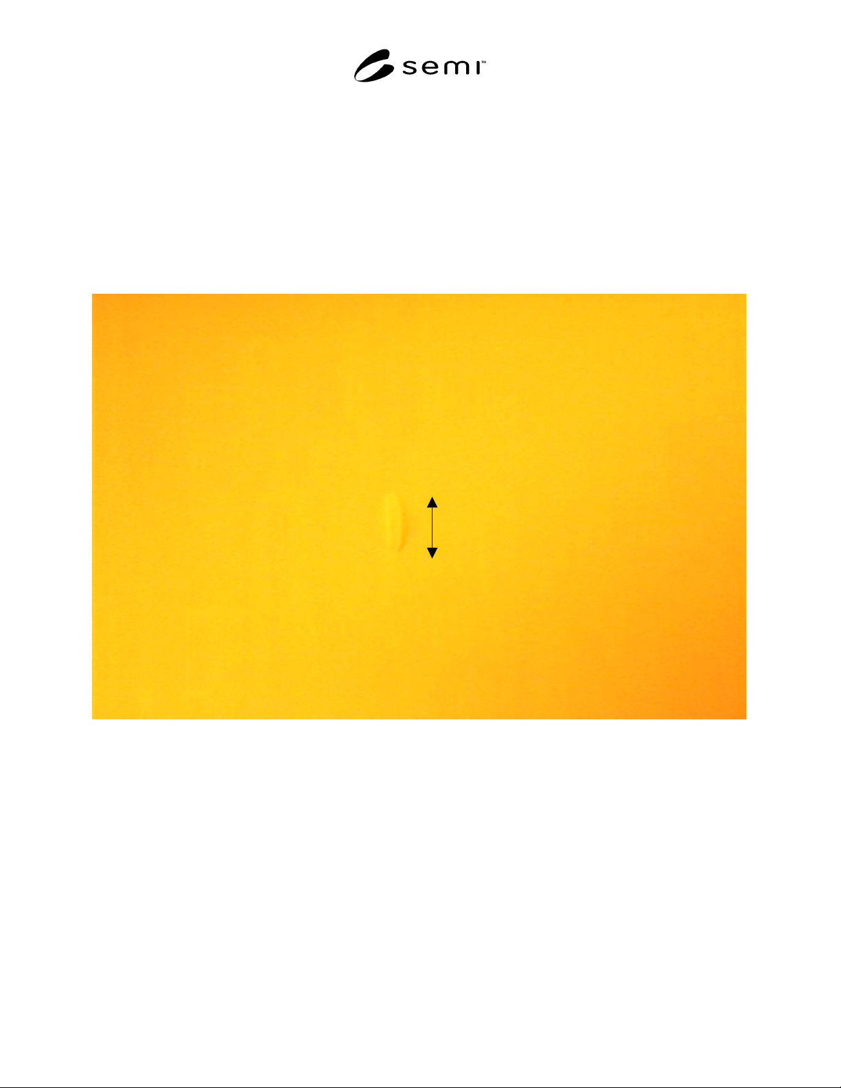
4.3.1 mound (epi) — a rounded protrusion on a
semiconductor wafer surface, which may have one or
more partially developed facets (see Figure 1).
1 American Society for Quality Control, 611 East Wisconsin Avenue,
Milwaukee, WI 53202. Website: www.asqc.org.
2 ISO Central Secretariat, C. P. 56, CH-1211 Genève 20,
Switzerland; Website: www.iso.ch; available in the U.S. from
American National Standards Institute, 11 West 42nd Street, 13th
Floor, New York, NY 10036 Website: www.ansi.org.
NOTE 1: Scattering event size reported by SSIS will differ
from the physical size of the object. The figure captions in
the examples highlight this fact. No useful method exists at
the present time to quantify this relationship (see Section
7.3.3.3)
4.3.1.1 Discussion — Related characteristics include
the following:
• Device characteristics that may be affected —
critical feature dimensions, lithographic equipment
focus, gate oxide integrity.
• Detection characteristics used for characterization
— mound height, diameter at 50% height.
• Discrimination characteristics used for
characterization — positive height: 10–100 nm, or
approximately 20% of the epi layer thickness;
diameter: 0.1–6 µm; circular symmetry.
• Specification characteristics used for wafer
qualification — number per wafer, mound height,
height to diameter.
4.3.2 epi stacking fault — a two dimensional effect that
results from a deviation from the normal stacking
sequence of atoms in a crystal. [SEMI MF154, SEMI
MF1727]
NOTE 2: Discrimination and specification characteristics are
given in this section to facilitate equipment development (see
Section 7.3.3.3) and are not intended for use in commercial
wafer specifications.
4.3.2.1 Discussion — Epi stacking faults are typically
linked together into squares in the case of {100}
oriented wafers, and triangles in the case of {111}
oriented wafers. Most stacking faults are nucleated at
the epi layer substrate boundary, though some have
been observed being nucleated further into the epi
growth process. Faults are aligned along specific
crystallographic directions. For {100} wafer the sides
of the faults are aligned along <110> directions. The
length of a side is typically proportional to the epi layer
thickness and related to the crystallographic orientation.
In order to minimize the strain around a stacking fault
contaminants may diffuse to these defects. Some
stacking faults may have an effect on the local growth
rate giving the stacking fault a three dimension aspect.
This three dimensional aspect changes their light
scattering cross section when observed by an SSIS (see
Figures 3 through 7). Still more complicated are
overlapping stacking faults which scatter even more
than a single stacking fault of the same size (see figure
4). Other types of defects may be composites of
stacking faults and polysilicon growth which can also
appear larger than a single stacking fault of the same
lateral dimensions (see Figures 5 and 6). Related
characteristics include the following:
SEMI M11-0704 © SEMI 1988, 2004 3
• Device characteristics that may be affected —
leakage and gate oxide integrity, from
crystallographic changes.
• Detection characteristics used for characterization
— side length and depth, orientation parallel to a
<110> direction.
• Discrimination characteristics used for
characterization — shape, length ~ epi layer
thickness: 1–10 µm. Stacking faults may cluster
(see Figure 7) and scatter more than a single
stacking fault.
• Specification characteristics used for wafer
qualification — Number per wafer. Since certain
types of epi stacking faults have no observed
impact on device performance while others are
killer defects no number can be assigned without a
clear identification of the type of epi stacking fault
that is involved.
Figure 1
A Mound. Magnification 1000 times using Nomarksi Interference Microscopy. Approximate SSIS scattering
event size 0.22 µm.
23 µm
SEMI M11-0704 © SEMI 1988, 2004 4
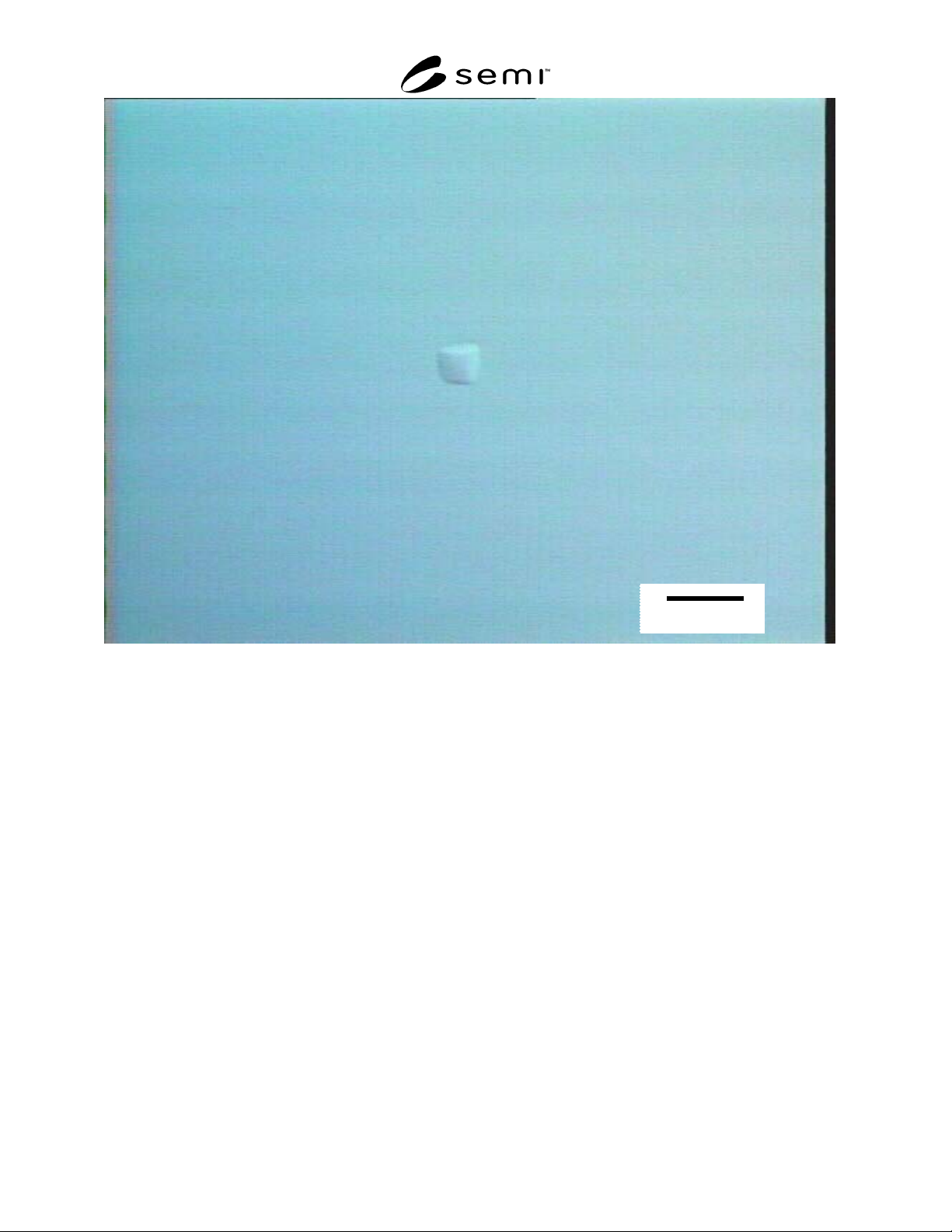
Figure 2
This is a mound that does not have the sharp edges of an Epitaxial Stacking Fault, but is not as high as a
Bump. They are typically sized much smaller in a SSIS than their actual size, but some have facets that
scatter enough light to be more easily detected. Some people refer to this feature as a hillock which is a type
of mound. The shape can be either circular or square. Magnification 500 times using Nomarski Interference
Microscopy. Approximate SSIS event size: 0.15 µm
20
µ
m