semi合集-English.pdf - 第7299页
SEMI MF1049-0304 © SEMI 2003, 2004 3 add 2 parts hy drofluoric acid (HF) to 1 part chromic acid solution a nd 1.5 parts water by volume. Pre pare and mix i n HF-proof beakers. 8.3.4 The specified chemical s shall have th…

SEMI MF1049-0304 © SEMI 2003, 2004 2
NOTICE: Unless otherwise indicated, all documents
cited shall be the latest published versions.
5 Terminology
5.1 Definitions
5.1.1 haze — on a semiconductor wafer, non-localized
light scattering resulting from surface topography
(microroughness) or from dense concentrations of
surface or near-surface imperfections.
5.1.1.1 Discussion — Haze due to the existence of a
collection of imperfections of the type that result in
haze cannot be readily distinguished by the eye or other
optical detection system without magnification. In a
scanning surface inspection system, haze and laser-light
scattering events comprise the laser surface scanner
signal due to light scattering from a wafer surface.
5.1.2 shallow etch pits — etch pits that are small and
shallow in depth under high magnification, >200×.
Also known as saucer pits.
6 Summary of Practice
6.1 Silicon wafers, either epitaxial or polished, are
thermally oxidized and preferential etched to reveal
small etch pits, shallow in depth, when observed
through an interference contrast microscope.
6.2 The distribution of the etch pits on the surface of
the wafer is determined and recorded on a diagram.
7 Apparatus
7.1 High-Intensity, Narrow-Beam Light Source —
Tungsten filament with a concentrated beam intensity
greater than 16 klx (1500 fc) and a beam diameter of 20
to 40 mm (0.8 to 1.6 in.) at a position 100 mm (4 in.)
from the light-source housing. The light beam shall not
be collimated and shall be capable of forming an image
of the bulb filament at the lamp focus length.
NOTE 3: Some standard microscope illuminators meet these
requirements.
7.2 Hydrofluoric Acid-Proof Chemical Laboratory
Apparatus — Fluorocarbon, polyethylene, or
polypropylene beakers, graduates, tweezers, eye
protection, apron, gloves, and protective sleeves.
7.3 Wafer Holders — HF acid-proof wafer carriers
which hold wafers. These are required if more than one
wafer is to be etched at a time.
7.4 Optical Microscope — Equipped with interference
contrast attachment. The eyepiece and objective lens in
combination shall give 200× to 1000× magnification.
NOTE 4: Nomarski differential interference contrast is an
example of interference contrast.
7.4.1 Stage Micrometer — With divisions of 0.002 mm
or finer, if an estimate of the shallow etch pit density is
to be made.
7.5 Acid Sink — A fume hood and facilities for
disposing of acids and their vapors.
7.6 Spin Dryer — Used to dry the wafers. Although
this item is not required, it is useful to provide a surface
free of residue artifacts.
8 Reagents and Materials
8.1 Purity of Reagents — Reagents for which SEMI
specifications have not been developed shall conform to
the specifications of the Committee of Analytical
Reagents of the American Chemical Society
4
. Other
grades may be used provided it is first ascertained that
the reagent is of sufficiently high purity to permit its
use without lessening the accuracy of the determination.
8.1.1 Hydrofluoric Acid (HF) — concentrated, in
accordance with Grade 1 of SEMI C28.
8.1.2 Nitrogen (N
2
) — 99.998% purity, in accordance
with Grade 4.8 of SEMI C59.
8.1.3 Oxygen (O
2
) — 99.98% purity, in accordance
with SEMI C54.
8.2 Purity of Water — Reference to water shall be
understood to mean Type E-3 or better water as
described in ASTM Guide D 5127.
8.3 Schimmel Etch for (100) and (111) Surfaces
5
8.3.1 Chromic Acid Solution — Make a 0.75 M
solution by placing 75 g of chromium trioxide (CrO
3
) in
a 1-L glass volumetric flask and then add sufficient
water to make a solution volume of 1 L, or 1000 mL.
The solution may be stored up to 6 months in clean
glass, TFE-fluorocarbon, polyethylene, or
polypropylene bottles.
8.3.2 For Test Specimens with Resistivity Greater Than
0.2
Ω
!cm n- or p-Type — Immediately before using,
add 2 parts hydrofluoric acid (HF) to 1 part chromic
acid solution by volume. Prepare and mix in HF-proof
beakers.
8.3.3 For Test Specimens with Resistivity Less Than
0.2
Ω
!cm n- or p-Type — Immediately before using,
4 Reagent Chemicals, American Chemical Society Specifications,
American Chemical Society, Washington, DC. For suggestions on the
testing of reagents not listed by the American Chemical Society, see
Analar Standards for Laboratory Chemicals, BDH Ltd., Poole,
Dorset, U.K., and the United States Pharmacopeia and National
Formulary, U.S. Pharmacopeial Convention, Inc. (USPC), Rockville,
MD.
5 Schimmel, D. G., “Defect Etch for 〈100〉 Silicon Evaluation,” J.
Electrochem. Soc., 126, 479–483 (1979).
SEMI MF1049-0304 © SEMI 2003, 2004 3
add 2 parts hydrofluoric acid (HF) to 1 part chromic
acid solution and 1.5 parts water by volume. Prepare
and mix in HF-proof beakers.
8.3.4 The specified chemicals shall have the following
nominal assay:
• Chromium trioxide >98.0%
• Hydrofluoric acid, concentrated 49 ± 0.25%
8.3.5 The chemicals used in this evaluation procedure
are potentially harmful and must be handled in an acid
exhaust fume hood, with utmost care at all times.
9 Sampling
9.1 Select wafers to represent the lot to be tested as
specified in producer-consumer agreements.
10 Specimen Preparation
10.1 In most instances this practice may be used for
polished or epitaxial wafers as they are received, but if
cleaning is required, the parties using this practice must
establish a mutually acceptable cleaning procedure
prior to etching.
11 Procedure
11.1 Handle wafers only with a clean, nonmetallic
pickup tool or automated transfer unit to avoid
scratching or contaminating the surface.
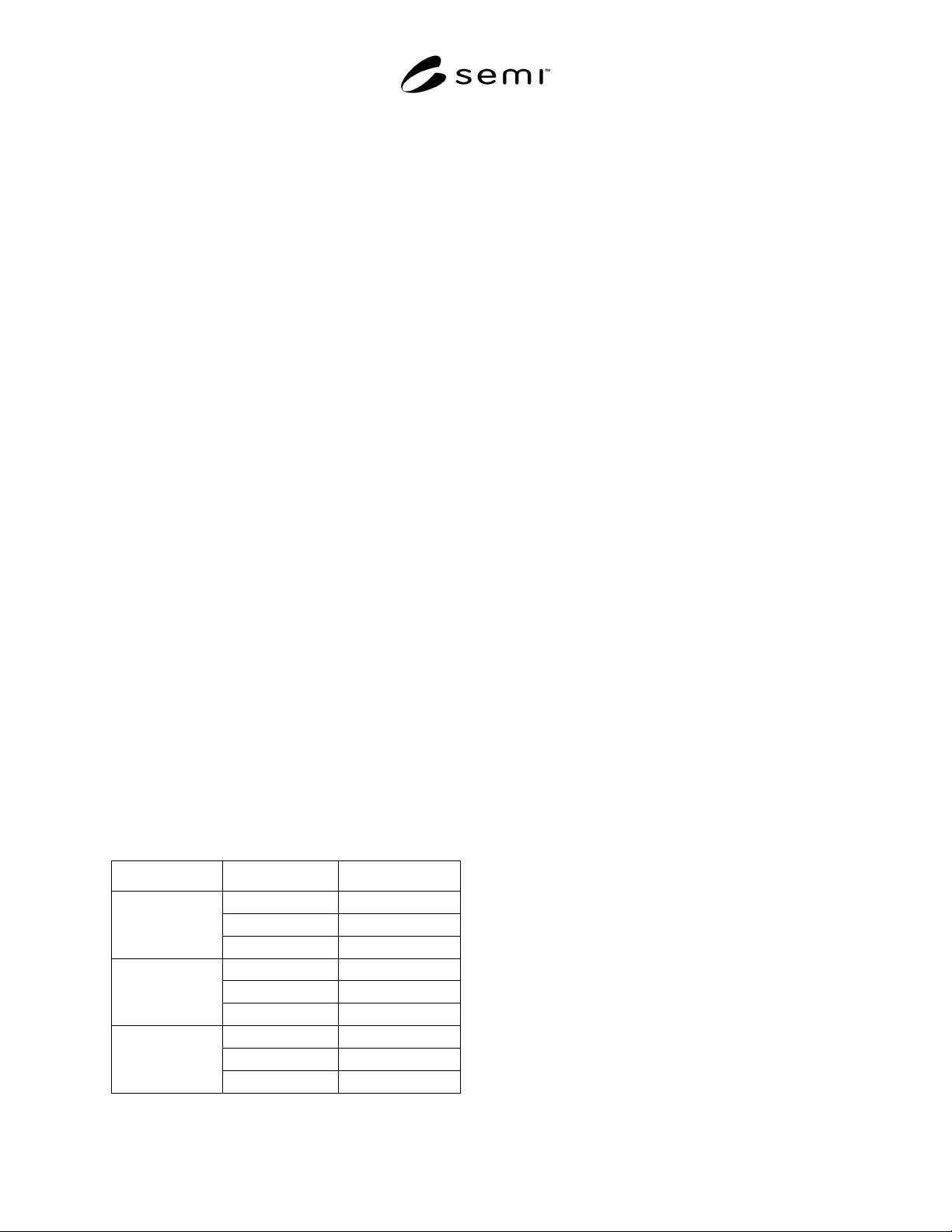
11.2 Oxidize the wafers by the thermal sequence listed
in Table 1.
NOTE 5: Large diameter furnaces may have difficulty in
duplication of this process. Rapid thermal processing is an
acceptable alternative.
11.2.1 Preheat the furnace to the push temperature.
11.2.2 Load the specimen wafers into the wafer boat,
being careful to avoid binding, scratching, or
contamination.
Table 1 Shallow Pit Oxidation Procedure
Step Function Conditions
Ambient 1% O
2
, 99% N
2
Temperature 950° C
Push (Load)
Push Rate 60 cm/min.
Ambient 1% O
2
, 99% N
2
Temperature 950° C
Oxidation
Time 7 min
Ambient 1% O
2
, 99% N
2
Temperature 950° C
Pull (Unload)
Pull Rate 60 cm/min.
11.2.3 Insert the boat into the hot zone at the rate called
for in Table 1. The wafer boat shall be centered in the
uniform hot zone.
11.2.4 Follow the oxidation and pull procedures as
specified in Table 1.
11.2.5 Because silicon wafers and quartz accessories
are extremely hot when they are removed from the
oxidation furnace, allow the materials adequate time to
cool before handling.
11.3 Transfer the room temperature wafers from the
quartz boat to a wafer holder using the pickup tool or
automated transfer unit.
11.4 Remove the thermal oxide layer using
hydrofluoric acid for 2 min followed by water rinse and
dry, using the spin dryer, if available.
11.4.1 Caution — Hydrofluoric acid solutions, used
here and for etching, are particularly hazardous and
specific preventive measures must be strictly observed.
Safety or protective gear should be worn while handling
acid solutions. Safety requirements vary, but the
essentials are: acid sink and personnel covering
including plastic gloves, safety glasses, face shield, acid
gown, and shoe covers. Hydrofluoric acid solutions
should not be used by anyone who is not familiar with
the specific preventive measures and first aid treatments
given in the appropriate Material Safety Data Sheet.
11.5 Etch the wafers for 2 minutes in an adequate
amount of Schimmel etch appropriate for the wafer
resistivity (see Sections 8.3.2 and 8.3.3). If the defect
etch pits are too small to distinguish, increase the etch
time up to 5 min.
11.5.1 Warning: Chromic acid, contained in the defect
etch solutions, should not be released into drains that
lead directly to domestic sewers. Chromates are an
extreme eco-hazard and must be first treated by reduc-
tion to the trivalent form. Chromic acid is a strong
oxidizing agent and should not be allowed to contact
organic solvents or other easily oxidized materials.
11.6 Quickly transfer the loaded wafer holder into a
water bath to rinse the wafers.
11.7 Dry the wafers, using the spin dryer, if available.
12 Evaluation
12.1 View the wafers at 1× magnification under the
high-intensity, narrow-beam light source in a dark
hood. If haze is observed, further examine the etched
wafer under a minimum of 200× magnification to
establish if the haze is due to shallow etch pits. If no
shallow etch pits are seen, record the wafer as being
free of shallow etch pits.
SEMI MF1049-0304 © SEMI 2003, 2004 4
NOTE 6: The percentage of the wafer covered may be
determined with the use of the universal wafer grid specified
in SEMI M17 that divides the wafer into 1000-area elements.
If the universal wafer grid is used, record the size of the edge
exclusion or the fixed quality area used. A1.6-mm peripheral
ring on a 125-mm diameter wafer represents 5% of the wafer
area.
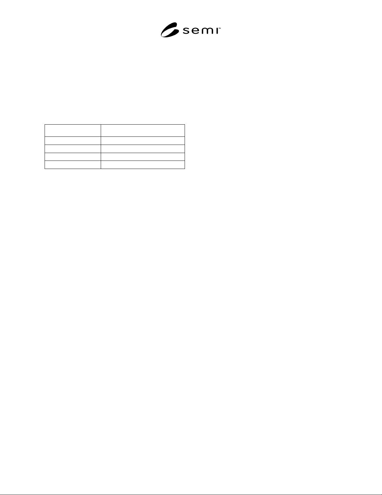
12.2 Determine the level of haze present on the surface
from Table 2.
Table 2 Haze Level Classification
Level % of Wafer Area
A 0–5
B 5–25
C 25–75
D 75–100
12.3 Optional Estimation of Shallow Etch Pit Density
— If it is desired to estimate the shallow etch pit
density, use the procedure in Related Information 1.
13 Report
13.1 Report the following information:
13.1.1 Date of test, laboratory and operator
identification,
13.1.2 Identification of wafer lot,
13.1.3 Identification of the test wafer(s) (including
conductivity type, orientation, diameter, growth
method, and back surface condition),
13.1.4 Level of haze for each wafer tested, and
13.1.5 A diagram showing the location and distribution
of areas of high shallow etch-pit density, and, if
estimates of shallow etch-pit density are made,
locations of the count positions.
13.2 If the shallow etch-pit density was estimated on
one or more wafers, also report the following
information of each wafer tested:
13.2.1 Magnification used in the test,
13.2.2 Average estimated shallow etch-pit density, and
13.2.3 Maximum and minimum measured shallow
etch-pit density, if more than one count position was
employed.
14 Keywords
14.1 epitaxial; oxidation; preferential etch; saucer pit;
shallow etch pit; silicon