semi合集-English.pdf - 第6222页
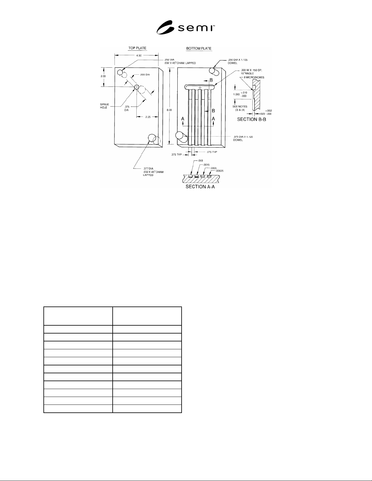
SEMI G45-93 © SEMI 198 6, 1993 3 Figure 1 Flash Test Mold 1. Hand Mold, Po lished, Very Well Mated Surfaces, Base Plates 0.75 thk . 2. Mold: C o mm o n Run ner Feeds Flash Channels of 0.003, 0.0015, 0.00 05, and 0.00025 …

SEMI G45-93 © SEMI 1986, 1993 2
5.3 At the beginning of each series of tests and at each
change of compound, check and set the transfer
pressure using the force gauge. The proper force gauge
setting can be determined from the formula:
F=
ΠD
2
P
4
where F is the force in pounds, P is the desired pressure
on the material in psi, and D is the ram diameter in
inches.
5.4
For each material change, make at least three clean
out runs using the material to be tested before recording
data. These runs may be used to determine the charge
weight.
5.5
Weigh out the compound to the nearest 0.1 g as
previously determined to yield a cull of 3.302 ± 0.254
mm (0.130 ± 0.010 in).
5.6
Raise the ram, add the compound to the pot, and
immediately activate the transfer cycle.
5.7
Remove cull and measure thickness. If the cull is
not within 0.130 ± 0.010 in, discard the run and repeat
the test, adjusting the charge weight as necessary.
5.8
Open mold and measure longe st flash for each
channel to nearest 0.25 mm (0.010 in) using 3×
minimum magnification. Be sure to check both top and
bottom plates of mold before measuring flash.
NOTE: Care must be taken to include the measurement of
transparent and semi-transparent flash which may be present
in the smaller channel. After measurements, diligence is
required to remove all flash, including the transparent and
semi-transparent varieties prior to the next test.
5.9 Repeat Steps 5.6 through 5.8 at least 3 times for
repeatability.
6 Reporting of Results
6.1 Report the material designation and lot number.
6.2 Report the average and standard deviation of the
flash length in each channel.
6.3 Report the temperature and pressure used for the
tests.
NOTE: Common Errors/Problems:
• Inadequate preheat of flash mold and/or transfer
plunger prior to test and between shots.
• Incorrect cull thickness.
• Omission of transparent or semi-transparent flash
in measurement (often present in smallest two
channels).
• Inadequate cleaning of mold between shots.
• Starting from the end of the ruler to make flash
length measurements instead of starting at a known
distance from the end.
• Inadequate mold break-in. Three shots should be
run and disregarded before recording flash
measurements for each material.
• Sprue, channel entry point, and mating mold
surface wear may produce error in measurement
and correlation problem. The impact of wear on
results has not been determined. Extent of
permissible mold wear requires agreement between
testing organizations.
SEMI G45-93 © SEMI 1986, 19933
Figure 1
Flash Test Mold
1. Hand Mold, Polished, Very Well Mated Surfaces, Base Plates 0.75 thk.
2. Mold: Common Runner Feeds Flash Channels of 0.003, 0.0015, 0.0005, and 0.00025 inches by 0.375 wide ±
0.00025.
3. Mold Flash Channels: Surface Finish 8 microinches
4. Mold Flash Channels Depth Tolerance:
a. ± 0.00005" for 0.00025 and 0.0005: Channels
b. ± 0.0002" for 0.0015 and 0.003 Channels
AUXILIARY INFORMATION
Conversions
Inches
Conversions
Millimeters
8.000 203.20
4.500 114.30
2.250 57.15
2.000 50.80
1.125 28.58
1.000 25.40
0.377 9.58
0.375 9.53
0.300 7.62
0.252 6.40
0.250 6.35

SEMI G45-93 © SEMI 1986, 1993 4
NOTICE: These standards do not purport to address
safety issues, if any, associated with their use. It is the
responsibility of the user of these standards to establish
appropriate safety and health practices and determine
the applicability of regulatory limitations prior to use.
SEMI makes no warranties or representations as to the
suitability of the standards set forth herein for any
particular application. The determination of the
suitability of the standard is solely the responsibility of
the user. Users are cautioned to refer to manufacturer’s
instructions, product labels, product data sheets, and
other relevant literature respecting any materials
mentioned herein. These standards are subject to
change without notice.
The user’s attention is called to the possibility that
compliance with this standard may require use of
copyrighted material or of an invention covered by
patent rights. By publication of this standard, SEMI
takes no position respecting the validity of any patent
rights or copyrights asserted in connection with any
item mentioned in this standard. Users of this standard
are expressly advised that determination of any such
patent rights or copyrights, and the risk of infringement
of such rights, are entirely their own responsibility.
Copyright by SEMI® (Semiconductor Equipment and Materials
International), 3081 Zanker Road, San Jose, CA 95134. Reproduction o
f
the contents in whole or in part is forbidden without express written
consent of SEMI.