semi合集-English.pdf - 第5783页
SEMI P23-0200 © SEMI 1993 , 2000 6 25, 000 u m 25, 000 u m 25 , 0 00 um 25 , 0 00 u m De f e ct Ch ip Re f e r en ce Chip 12, 500 um L i g h t A d ju s t m e n t P a tt e r n 12 , 5 00 um S EMI S T AN DARD P23- 0200- 15 …

SEMI P23-0200 © SEMI 1993, 20005
10.3.4.2 Contact Hole Pattern
10.3.4.2.1 As with Edge Intrusion in 10.3.2, Defect
Size is S2.
10.3.5 Over Size
10.3.5.1 Wiring Pattern
10.3.5.1.1 Since size only changes in the Y-direction,
Defect Size is (d-c).
10.3.5.2 Contact Hole Pattern
10.3.5.2.1 With “a” and “c” as the reference pattern
size, Defect Size is (b-a) or (d-c), whichever is larger.
10.3.6 Under Size
10.3.6.1 Wiring Pattern
10.3.6.1.1 Since size only changes in the Y-direction,
Defect Size is (d-c).
10.3.6.2 Contact Hole Pattern
10.3.6.2.1 With “a” and “c” as the reference pattern
size, Defect Size is (b-a) or (d-c), whichever is larger.
10.3.7 Elongation & Truncation
10.3.7.1 Since, in a program defect, the size only
changes in the Y-direction (S1), Defect Size is S1.
10.3.8 Misplacement
10.3.8.1 Since the program defect is only moving
along the Y-axis, Defect Size is Y.
10.3.9 Missing Pattern
10.3.9.1 With S1 and S2 as the reference pattern size,
Defect Size is S1 or S2, whichever is larger.
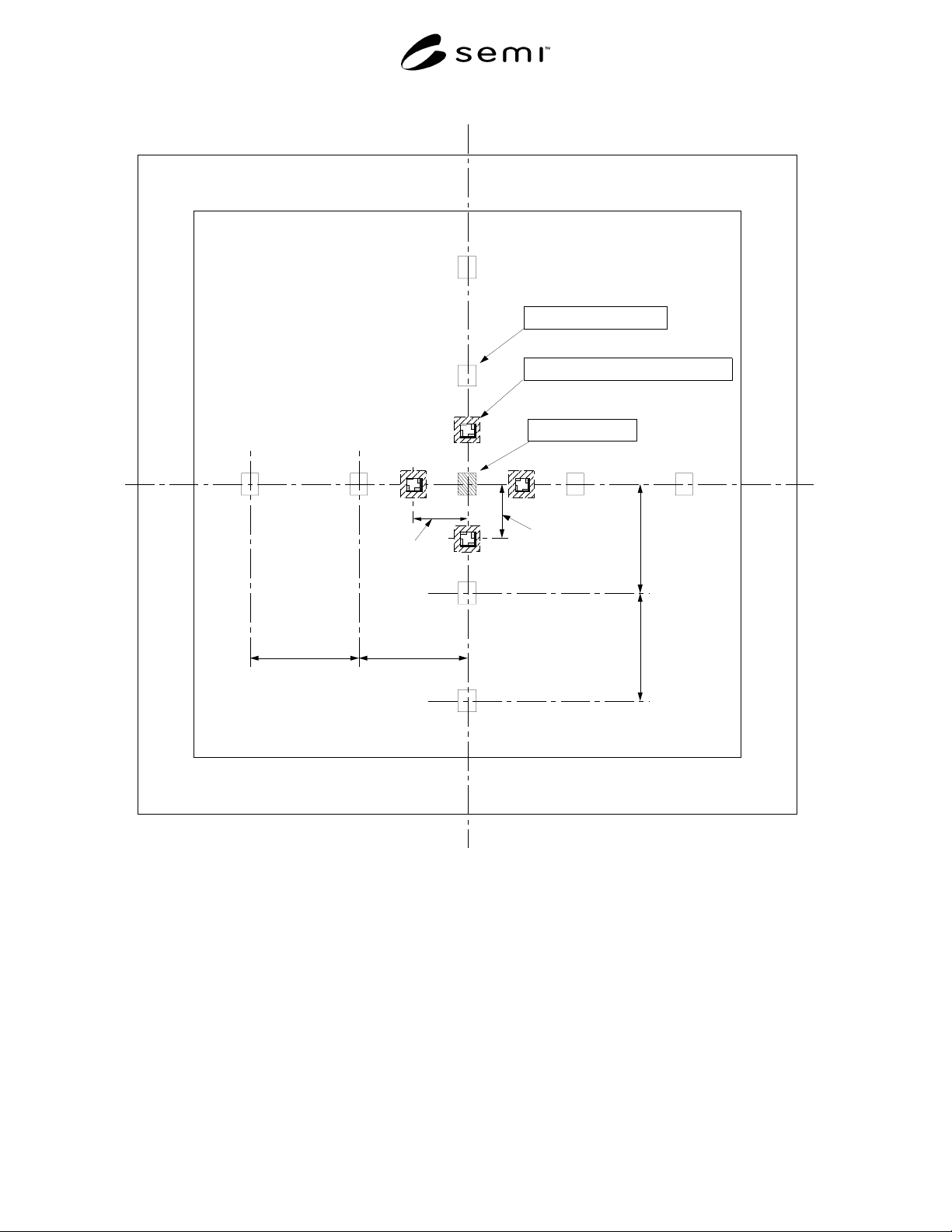
11 Light Intensity Adjustmen t Pattern
11.1 Light intensity adjustment patterns will be placed
in four areas in mask defect inspection systems. (See
Figure 1.)
11.2 A glass pattern will be placed in the center.
11.3 Around the circumference of the glass pattern, a
line and space pattern will be placed, 1 for 1, with the
same line width as the design rule (dimensions on
mask).
11.3.1 With 500 by 1,250 microns as one block, place
horizontal patterns on the left and right sides,
perpendicular patterns on the top and bottom. Also,
place a horizontal pattern on the lower left corner.
(See Figure 25.)
11.4 The circumference of the glass pattern and line &
space pattern should have at least 6,000 microns of
shade film.
12 Method for Use of Test Masks in
Evaluating Mask Defect Inspection System
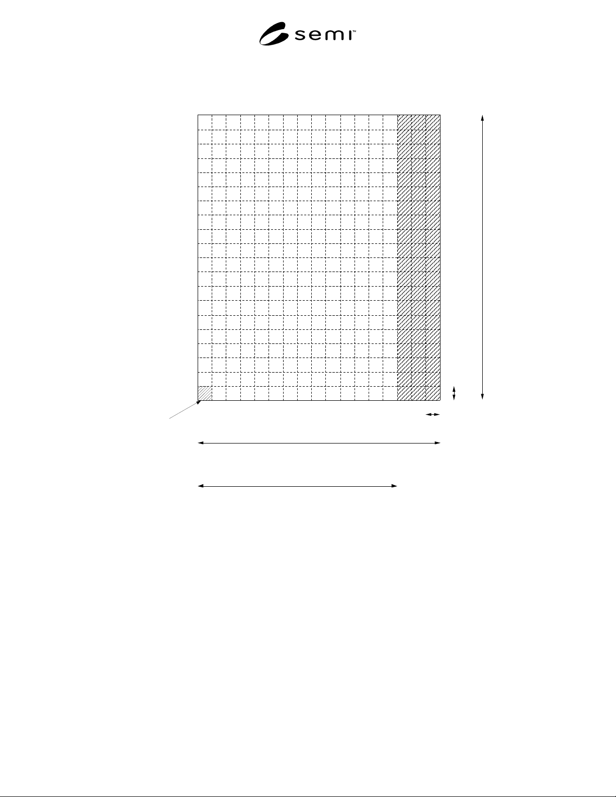
12.1 Inspect all defect cells, or a portion of them
according to the inspection conditions of the mask
defect inspection system to be evaluated.
12.2 Perform at least 20 inspections.
12.3 Perform the inspection at least with a set
direction of 0º. It is also preferable that the inspection
be performed after rotating the set at 90º, 180º, and
270º.
12.4 When displaying the defect inspection sensitivity
for mask defect inspection system, display the defect
size of the smallest defect of each type which was
detected 100%. (See Figures 26 and 27.)
SEMI P23-0200 © SEMI 1993, 2000 6
25,000 um 25,000 um
25,000 um25,000 um
Defect Chip
Reference Chip
12,500 um
Light Adjustment Pattern
12,500 um
SEMI STANDARD
P23- 0200- 1500C
or
(P23- 0200- 1500W)
5inch Mask
6inch Mask
Figure 1
Mask
SEMI P23-0200 © SEMI 1993, 20007
Cel l
QPONMLKJIHGFEDCBA
Defect T ype
01
02
03
04
05
06
07
08
09
10
11
12
13
14
15
16
17
18
19
20
Defect Number
0.75
0.70
0.65
0.60
0.55
0.50
0.45
0.40
0.30
0.35
0.20
0.25
0.15
0.10
0.05
0.80
0.90
1.00
0.85
0.95
Defect Design Size (um)
250 um
4,250 um (Wiring)
250 um
5,000 um
3,500 um (Contact Hole)
Figure 2
Chip
Wiring Chip; A to Q (#340 cell)
Contact Hole Chip; A to N (#280 cell)