semi合集-English.pdf - 第4039页
SEMI F51-0200 © SEMI 2000 5 Categories fo r Consideratio n LIQUID CHEMI CALS CORROSIVES OXIDIZ ERS SOLVENTS Figure 2 Liquid Che mical Chart Categories fo r Consideratio n THERM AL ION IMPLANT (Hi V ac) RTP LPCVD ATM ATM …
SEMI F51-0200 © SEMI 2000 4
that the seals not only be capable of withstanding these
high temperatures but also that they not out-gas or
permeate adversely affecting the purity of the process.
Also of concern is the possible particle generation
caused by the seals as they expand and contract due to
temperature cycling (see Section 8.4.1).
9.1.1 Factors include:
• Temperature capability of material and process
temperature.
• Static or dynamic state of seal.
• Proper sizing and fit of seal to gland.
10 Considerations for Use in Plasma Systems
(Etch, CVD, and PVD)
NOTE 5: See Figure 4.
10.1 Considerations for sealing components for use in
plasma applications shall include proximity to plasma,
plasma reactor temperature, chemical composition of
plasma, plasma energy, and chemical leaching by the
plasma.
10.2 Contamination from the inhere nt seal
components and particle generation is directly related to
other considerations mentioned above.
10.2.1 Factors include:
• Seal composition and resistance to chemical attack.
• Proximity to source and intensity of RF.
• Temperature capability of material and process
temperature.
• Static or dynamic state of seal.
• Proper sizing and fit of seal to gland.
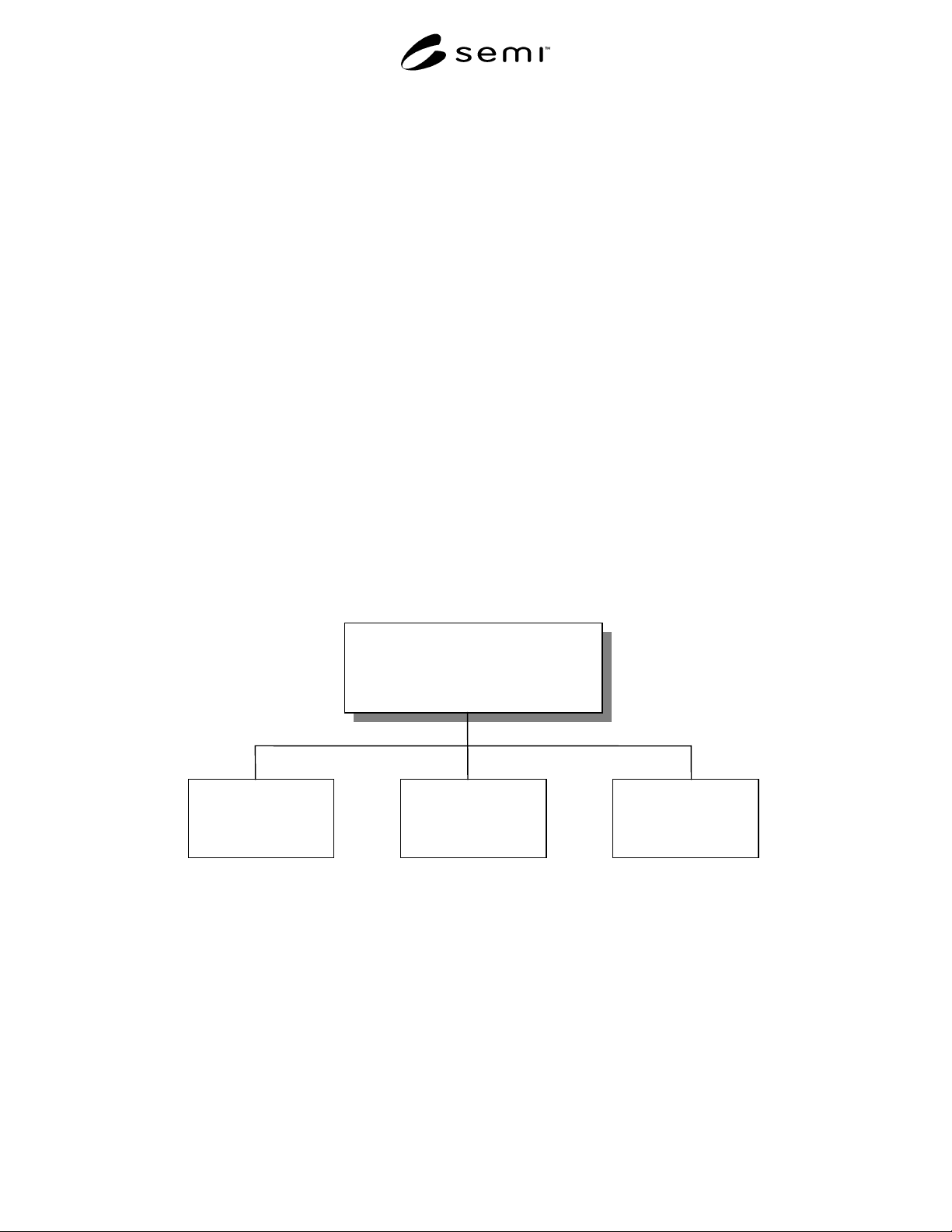
Categories for Consideration
UPDI
Chemical Thermal Radiation
Figure 1
UPDI Chart
SEMI F51-0200 © SEMI 20005
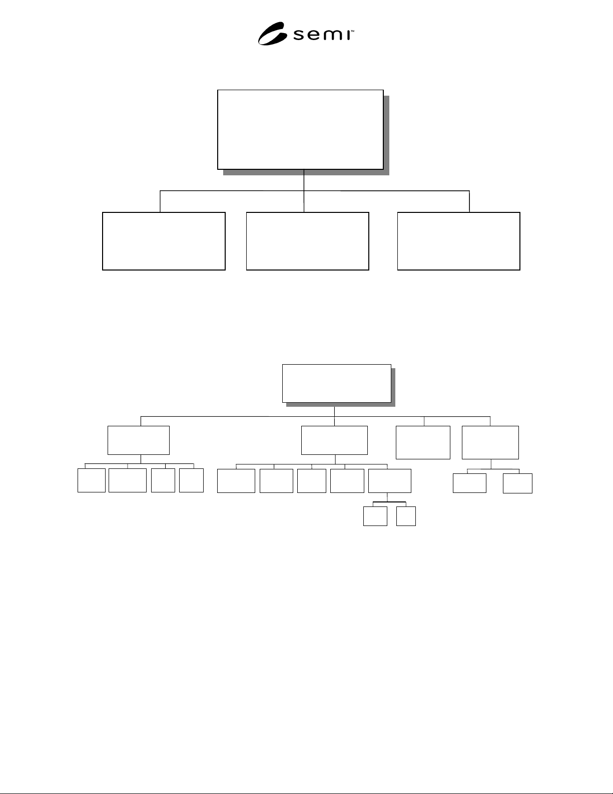
Categories for Consideration
LIQUID
CHEMICALS
CORROSIVES OXIDIZERS SOLVENTS
Figure 2
Liquid Chemical Chart
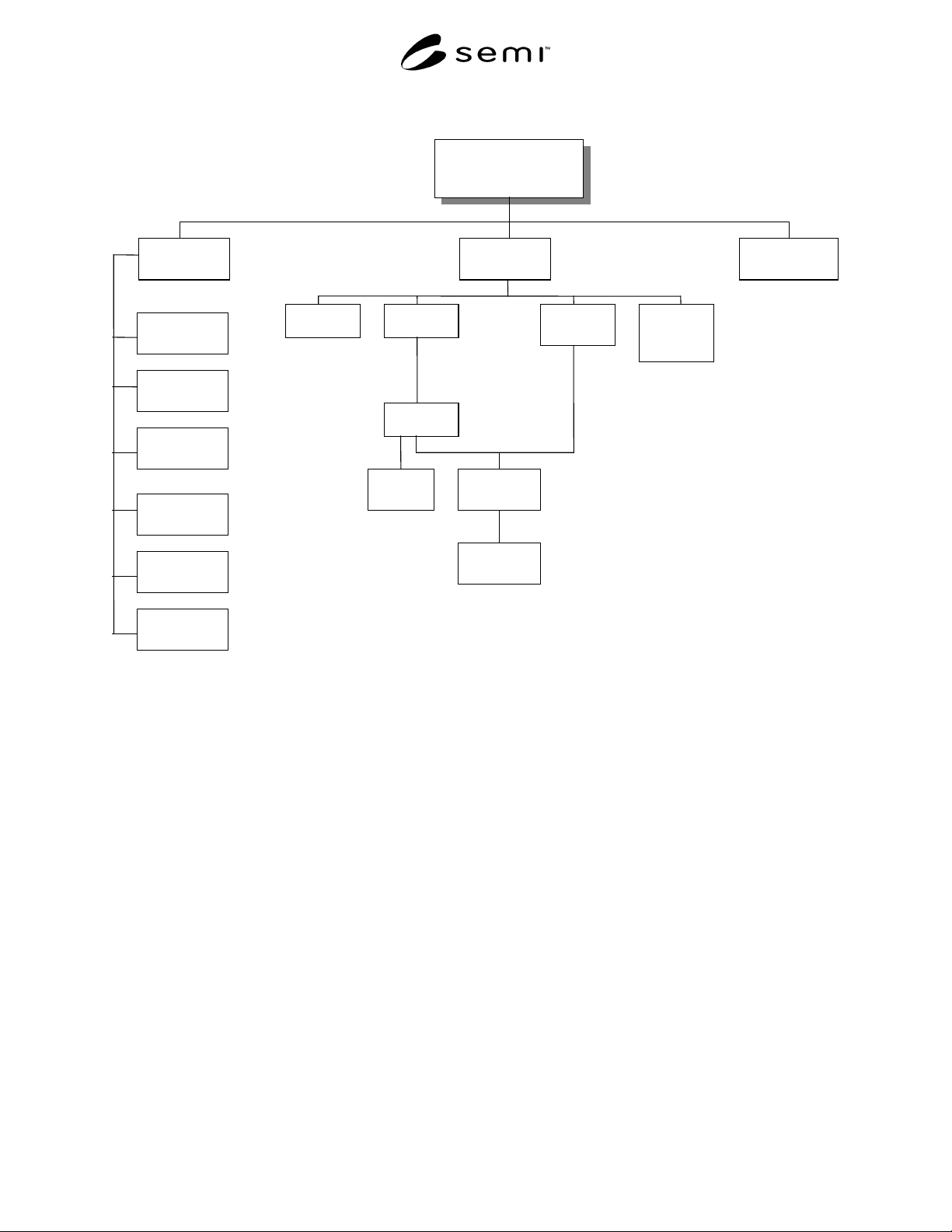
Categories for Consideration
THERMAL
ION
IMPLANT
(Hi Vac)
RTPLPCVDATM
ATM
POCI
3
O
2
,
N
2
CI
MOCVDTEOSNITPOLY
LTO,
HTO
TiN W
H
2
O
CVD
Figure 3
Thermal Chart
SEMI F51-0200 © SEMI 2000 6
Categories for Consideration
PLASMA
CVD
SiN
OxideHDP
PSG,
BPSG
BSG
ETCH
PVD
(Hi Temp)
TEOS
Cleaning
Tech
C
2
F
6
,
NF
3
F
Cl
Br
O
2
H
x
C
y
H
2
BPSG
BSG
Figure 4
Plasma Chart
NOTICE: SEMI makes no warranties or representations as to the suitability of the guides set forth herein for any
particular application. The determination of the suitability of the guide is solely the responsibility of the user. Users
are cautioned to refer to manufacturer’s instructions, product labels, product data sheets, and other relevant literature
respecting any materials mentioned herein. These guides are subject to change without notice.
The user’s attention is called to the possibility that compliance with this guide may require use of copyrighted
material or of an invention covered by patent rights. By publication of this guide, SEMI takes no position respecting
the validity of any patent rights or copyrights asserted in connection with any item mentioned in this guide. Users of
this guide are expressly advised that determination of any such patent rights or copyrights, and the risk of
infringement of such rights, are entirely their own responsibility.
Copyright by SEMI® (Semiconductor Equipment and Materials
International), 3081 Zanker Road, San Jose, CA 95134. Reproduction o
f
the contents in whole or in part is forbidden without express written
consent of SEMI.