semi合集-English.pdf - 第6468页
SEMI G78-0699 © SE MI 1999 1 SEMI G78-0699 TEST METHOD FOR COMPARING AUTOMATED WAFER PROBE SYSTEMS UTILIZING PROCE SS-SPECIFIC MEA SUREM ENTS This te st method w as technica lly approved by the Globa l Autom ated Test Eq…
SEMI G77-0699 © SEMI 1999 8
Symbol Value Specified Datum Measured From Feature Measured To
z41 1 mm
minimum
horizontal datum plane bottom of frame cassette
z43 1 + 0 -1 mm horizontal datum plane bottom rails
z47‡ 210 ± 1 mm
13-frame frame cassette
330 ± 1 mm
25-frame frame cassette
horizontal datum plane bottom of robotic handling flange
z48‡ 15 mm
minimum
bottom of robotic handling flange encroachment of frame cassette top
underneath robotic handling flange
z49‡ 8 mm
maximum
bottom of robotic handling flange top of robotic handling flange
† These dimensions match those of SEMI E1.9 with the same symbol.
‡ These dimensions match those of SEMI E47.1 with the same symbol.
NOTICE: These standards do not purport to address
safety issues, if any, associated with their use. It is the
responsibility of the user of these standards to establish
appropriate safety and health practices and determine
the applicability of regulatory limitations prior to use.
SEMI makes no warranties or representations as to the
suitability of the standards set forth herein for any
particular application. The determination of the
suitability of the standard is solely the responsibility of
the user. Users are cautioned to refer to manufacturer’s
instructions, product labels, product data sheets, and
other relevant literature respecting any materials
mentioned herein. These standards are subject to
change without notice.
The user’s attention is called to the possibility that
compliance with this standard may require use of
copyrighted material or of an invention covered by
patent rights. By publication of this standard, SEMI
takes no position respecting the validity of any patent
rights or copyrights asserted in connection with any
item mentioned in this standard. Users of this standard
are expressly advised that determination of any such
patent rights or copyrights, and the risk of infringement
of such rights, are entirely their own responsibility.
Copyright by SEMI® (Semiconductor Equipment and Materials
International), 3081 Zanker Road, San Jose, CA 95134. Reproduction o
f
the contents in whole or in part is forbidden without express written
consent of SEMI.

SEMI G78-0699 © SEMI 19991
SEMI G78-0699
TEST METHOD FOR COMPARING AUTOMATED WAFER PROBE
SYSTEMS UTILIZING PROCESS-SPECIFIC MEASUREMENTS
This test method was technically approved by the Global Automated Test Equipment Committee and is
the direct responsibility of the North American Automated Test Equipment Committee. Current edition
approved by the North American Regional Standards Committee on December 18, 1998. Initially
available at www.semi.org April 1999; to be published June 1999.
1 Purpose
1.1 To define the terms and provide a means of
comparative, or relative measurement for the automated
wafer prober functions: Accuracy, Repeatability and
Throughput.
2 Scope
2.1 This method may be used to evaluate the
performance of a single automated wafer prober, or as a
means to compare many probers. The probers that this
document addresses are defined as fully automated; that
is, having automatic material handling, alignment and
probing capabilities.
3 Limitations
3.1 This test and comparison meth od is not intended to
represent a statistically complete methodology for
measuring the performance of an automated wafer
prober. Its correct use is a practical means to compare
the stepping capabilities of wafer probers within a
specific end user’s environment.
3.2 The definitions of the terms “Repeatability” and
“Accuracy” as used in this document are not in
accordance with those of the National Conference of
Standards Laboratories (NCSL) nor are they intended to
be. They are to be used solely for the purpose of this
document and have no other intended uses.
3.3 It is difficult to characterize an d eliminate high
temperature contributions to positional error such as
probe needle ‘float’. Therefore, it is strongly
recommended that the same probe card be used to
evaluate all of the probers being considered.
3.4 It is recommended that the pro be card is verified to
be in the same condition (i.e. evaluated for positional
accuracy and overall functional condition) both before
and after the conclusion of each test.
3.5 Bump placement on a semiconductor device is
generally located ± 0.001" with respect to their nominal
location. Vertical probe cards used to probe bumps
have an inherent amount of needle drift. Therefore care
must be exercised in using vertical probe cards on
bump devices as a means of prober accuracy
measurement.
4 Referenced Documents
NOTE: As listed or revised, all documents cited shall be the
latest publications of adopted standards.
4.1 SEMI Documents
SEMI E10 — Standard for Definition and Measurement
of Equipment Reliability, Availability and
Maintainability (RAM)
SEMI S2 — Safety Guidelines for Semiconductor
Manufacturing Equipment
5 Terminology
5.1 3
σ
limit — a statistically deriv ed measurement of
process variation. A process that allows a ± 3σ
deviation will allow 2.7 parts per thousand to be outside
the established bounds.
5.2 accuracy — the ability of an a utomatic wafer
prober to index its chuck, and attached wafer, from an
initial position to a subsequent position and make
contact with a static probe tip at a nominal location on
the wafer. In the context of this method, accuracy is
defined as average die offset.
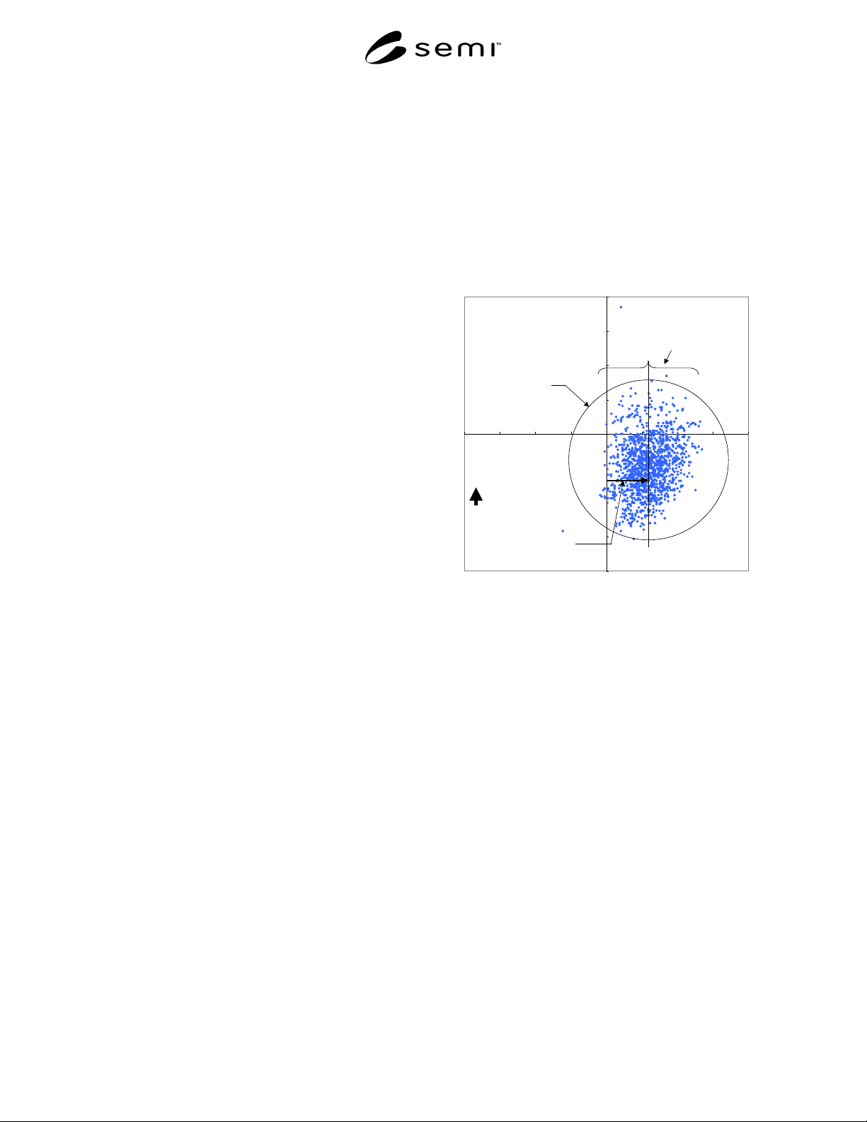
5.2.1 Average die offset is the perpe ndicular distance
measured from the centerline of the die pad to a parallel
line that statistically represents the scrub mark data
point distribution center (see Figure 1). Each data point
shown in this figure represents only the center value of
accumulated scrub marks produced by operation of this
method.
5.2.2 It should be noted that accuracy established by
this method is characteristic of the system, which in
total represents both the automated prober as well as its
probe card. Finally, this method establishes two
accuracy values, a value for pads along the X and Y
axes of the die. These axis directions are arbitrary.
5.2.3 It should be noted that if fully automated prober
set-up modes are not used for probe-needle-to-pad
alignment during testing, the possibility of operator
error should be considered as a variable when
evaluating system accuracy.
5.3 automatic wafer prober — device that
automatically and repeatedly aligns the die bonding
SEMI G78-0699 © SEMI 1999 2
pads or interconnect bumps on a semiconductor device
to a set of test needles attached to a probe card.
5.4 bonding pad — exposed metal lic contact area on a
semiconductor device that is surrounded by dielectric
passivation. This is the point at which a temporary
interconnect is made for wafer level test, and permanent
interconnect for packaging.
5.5 bumps — metallic elevated co ntact area on a
semiconductor device that is used in place of a bonding
pad. A die that is designed to use this type of
connection is commonly called a ‘flip chip’ or direct
chip attach.
5.6 die — individual semiconduct or device. For the
purposes of this method, the dice have not been
singulated, and are still in the form of a wafer. Used
interchangeably (in the context of wafer sort) with the
acronym DUT (Device Under Test).
5.7 overdrive — distance in Z whi ch the wafer is
driven beyond a user defined initial contact point,
typically ‘first electrical contact’.
5.8 overhead test — semiconducto r test method where
the test head is mounted directly over the prober, with
the goal of shortening the distance between the pin
electronics and the probe card. The connection
between the test head and the prober is generally
through a device called a Prober Tester Interface (PTI)
5.9 pin electronics — tester hardware that creates the
test signals used to challenge the DUT.
5.10 probe card — printed wiring b oard or ceramic
substrate with permanently attached needles or contacts
that are aligned at the time of manufacture to match the
contact pattern on a Die. Common types of probe cards
are:
• Blade
• Peripheral / Cantilever (AKA Epoxy Ring)
• Vertical (AKA Area Array or Cobra™)
5.11 probe card planarity and alignment — a user-
specified position of the probe tips in ‘x’, ‘y’ and ‘z’.
5.12 probe needles — the contact p oints between the
probe card and the bonding pads. These are typically
manufactured from one of the following materials:
• Beryllium copper
• Tungsten
• Tungsten-rhenium alloy
• Paliney
5.13 prober tester interface (PTI) — signal-
transmitting electro-mechanical device that connects
the pin cards in the tester to the probe card.
5.14 repeatability — Figure 1 is em pirical data and
represents a statistically significant sample of scrub
marks. This data reveals that probe needles may not
make contact consistently to the same point die to die.
Recall that accuracy is defined in this method as
average die offset. Thus, repeatability simply represents
the three-sigma distribution value for average die offset.
Repeatability will represent 99.7% or a three-sigma
distribution value for the accumulated offset data points
obtained through use of this method.
-20
-15
-10
-5
0
5
10
15
20
-20 -15 -10 -5 0 5 10 15 20
microns
microns
Repeatability
A
ccuracy
Average
approximation of
data points
Raw X-data
Direction of the
probe needle
Figure 1
Raw X-Data
5.14.1 The X-Y plotted centroids of these scrub marks
will be found to form a “cloud” of points, densest in the
center, and thinning out towards the edges.
5.14.2 Repeatability is the radius of th at cloud or
“cluster” of probe marks, as defined by the 3 σ or other
user defined limit of that cloud. The error in the
placement of the center of that cloud, relative to its
nominal target, is defined as the automatic wafer
prober’s “Accuracy”. (See Figure 1)
5.15 set point — the value to which a control system’s
input device has been set, as opposed to the actual value
to which the control system has driven the controlled
variable. For example, the input setting to the wafer
chuck temperature controller, as opposed to the actual,
independently measured temperature of the wafer
chuck.
5.16 soak time — time between a piece of equipment’s
reaching the set point temperature and use of that piece
of equipment.