semi合集-English.pdf - 第4878页
SEMI M2-1103 © SEMI 1985, 2003 4 9 Certification 9.1 Upon re quest of the purchaser in the cont ract or order, a manufact urer’s or suppl ier’s certifi cation that the material was manufacture d and tested in accordance …
SEMI M2-1103 © SEMI 1985, 2003 3
NOTE 4: Care should be taken in converting between carrier
density and resistivity using SEMI MF723. Multiple
conversions may introduce differences in values. For
example, converting from carrier density (C
i
) to resistivity
and back to carrier density (C
f
), may result in C
i
not equaling
C
f
.
6 Requirements
6.1 The substrate shall conform to SEMI M1 and to the
appropriate polished silicon wafer standard.
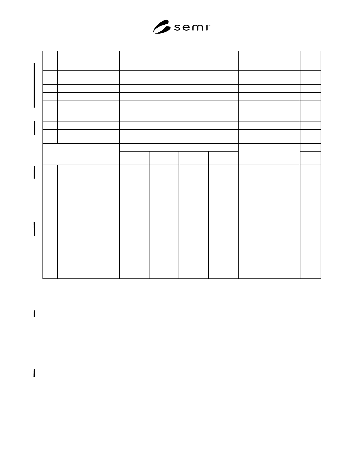
6.2 Epitaxial wafer defects shall not exceed the limits
as given in Table 1.
NOTE 5: When an unetched wafer is observed for slip, it is
impossible to differentiate between slip and linear misfit lines.
6.3 Layer Thickness Variation — Unless otherwise
specified, the radial thickness variation shall be
determined from values measured at the center and half
radius (R/2) locations, on diameters both parallel and
perpendicular to the primary flat, and shall be ≤ 6%
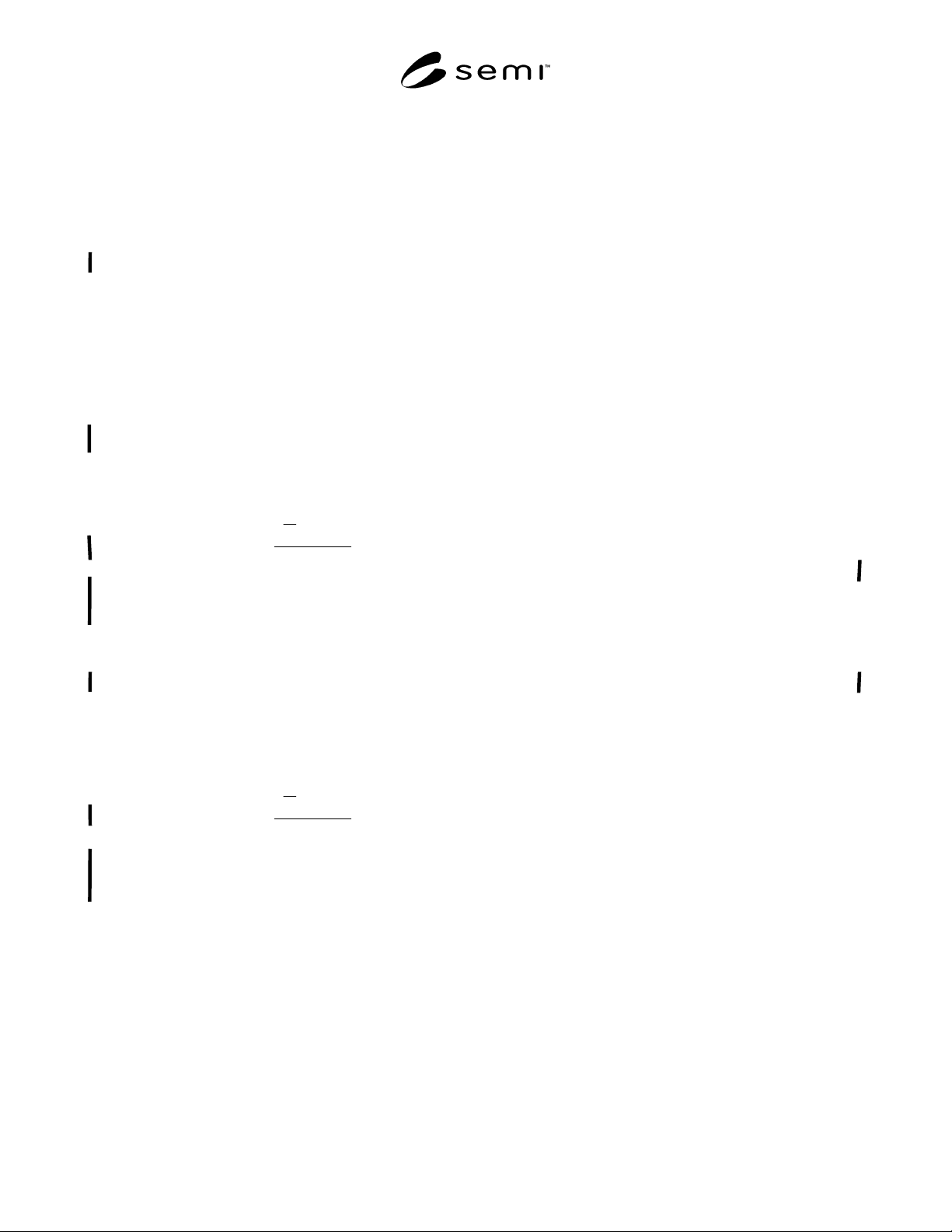
defined as follows:
100
2
(%)Variation
max
×
−
=
C
C
R
(2)
where R/2 denotes one of the layer thickness values
measured at half radius and C denotes the value at the
center point.
6.4 Net Carrier Density Variation — The radial net
carrier density variation shall be determined from
values measured at the center and half radius (R/2)
locations, on diameters both parallel and perpendicular
to the primary flat, and shall be ≤10% for net carrier
density ≥1 × 10
15
cm
-3
and ≤15% for net carrier density
<1 × 10
15
cm
-3
defined as follows:
100
2
(%)Variation
max
×
−
=
C
C
R
(3)
where R/2 denotes one of the net carrier density values
measured at half radius and C denotes the value at the
center point.
7 Sampling
7.1 Unless otherwise specified, appropriate sample
sizes shall be selected from each lot according to
ANSI/ASQC Z1.4. Each quality characteristic shall be
assigned an acceptable quality level (AQL) in
accordance with ANSI/ASQC Z1.4. Inspection levels
shall be agreed upon between supplier and purchaser.
7.2 Unless otherwise specified, the following AQL’s
shall be assigned:
7.2.1 Epitaxial layer thickness, 6.5%,
7.2.2 Epitaxial layer net carrier density, 6.5%,
7.2.3 Epitaxial wafer defects, cumulative, 4.0%.
8 Test Methods
8.1 Measurements shall be carried out in conformance
with the specified SEMI methods. Where no methods
are specified or where choices are given, the supplier
and purchaser shall agree in advance on the means for
making the measurement.
8.2 Substrate — Determine in accordance with
methods defined in SEMI M1.
8.3 Epitaxial Layer
8.3.1 Thickness — Determine in accordance with
SEMI MF95 or SEMI MF110.
NOTE 6: There is a possibility that various types of infrared
reflectance instrumentation may result in different values of
epitaxial layer thickness. Therefore, the instrumentation used
shall be agreed upon between supplier and purchaser.
8.3.2 Net Carrier Density — Determine by method(s)
agreed upon between supplier and purchaser.
NOTE 7: SEMI MF1392 and SEMI MF1393 are methods
for measuring net carrier density using a mercury probe
contact. If resistivity is measured, as by SEMI MF374 or
SEMI MF525, conversion to dopant density shall be made
using SEMI MF723. Net carrier density of very heavily doped
layers (or substrates) may be found using SEMI MF398. Net
carrier density profiles may be determined directly in
accordance with SEMI MF1392 or SEMI MF1393 or
indirectly in accordance with SEMI MF672, with conversion
from resistivity to net carrier density in accordance with
SEMI MF723. If the method used for determining the net
carrier density profile is not the same as that used to
determine the center point net carrier density, correlation
between the two methods used shall be established.
8.3.3 Epitaxial Wafer Defects — Determine in
accordance with the methods given in Table 1.
8.3.3.1 Surface inspection shall be performed before
any other testing. Wafers may be cleaned prior to
inspection to minimize difficulty in the visual
inspection of defects other than foreign matter.
8.3.3.2 Inspection for slip shall be done using grid
elements constructed in accordance with SEMI M17.
An element is defective if it contains one or more slip
lines. The total number of defective elements shall be
less than or equal to n, where n is listed in Table 1.
8.4 If substrates of different type and net carrier
density than the product substrates are to be used for
deposition control, their type, net carrier density, and
quantity per run or lot shall be agreed upon between
supplier and purchaser.

SEMI M2-1103 © SEMI 1985, 2003 4
9 Certification
9.1 Upon request of the purchaser in the contract or
order, a manufacturer’s or supplier’s certification that
the material was manufactured and tested in accordance
with this specification, together with a report of the test
results, shall be furnished at the time of shipment.
9.2 The user and supplier may agree that the material
shall be certified as “capable of meeting” certain
requirements. In this context, “capable of meeting”
shall signify that the supplier is not required to perform
the appropriate tests in Section 8; however, if the user
performs the test and the material fails to meet the
requirement, the material may be subject to rejection.
10 Packing and Package Labeling
10.1 Special packing requirements shall be subject to
agreement between the supplier and the purchaser.
Otherwise, all wafers shall be handled, inspected, and
packed in such a manner as to avoid chipping,
scratches, and contamination, and in accordance with
the best industry practices to provide protection against
damage during shipment.
10.2 The wafers supplied under these specifications
shall be identified by appropriately labeling the outside
of each box or container, and each subdivision thereof,
in which it may reasonably be expected that the wafers
will be stored prior to further processing. Identification
shall include supplier’s name and reference number,
purchaser’s P.O. number, quantity, dopant, orientation,
conductivity type of substrates and epitaxial layers,
carrier density (or resistivity, if so specified in the
purchase order or contract), and thickness of the
epitaxial layer. The reference number assigned by the
supplier shall provide ready access to information
concerning the fabrication history of the particular
wafers in that lot. Such information shall be retained on
file at the manufacturer’s facility for at least one year
after the particular lot has been shipped.
SEMI M2-1103 © SEMI 1985, 2003 5
Table 1 Discrete Epitaxial Wafer Defect Limits
Item Characteristics Maximum Limit Test Method Notes
1 Stacking Faults 15 per cm
2
SEMI MF1726 1
2 Slip n = 36 grid elements SEMI M17 and SEMI
MF1726
1, 2, 3
3 Haze NONE SEMI MF523 Section 12.2 1, 4, 5
4 Scratches NONE SEMI MF523 Section 12.2 1, 5, 6
5 Edge Chips NONE SEMI MF523 Section 12.2 7
6 Edge Crown Projection above wafer surface not to exceed 1/3 of
epi layer thickness
To be defined 2, 8
7 Foreign Matter NONE SEMI MF523 Section 12.3 1, 4
8 Back Surface
Contamination
NONE SEMI MF 523 Section 12.4 1, 4
Epitaxial Layer Thickness Front Surface
Characteristics Dependent on
Layer Thickness
< 25 µm 25–50 µm 50–100 µm > 100 µm
9 Large Point Defects
(Density per m
2
)
700 900 1200 1500 SEMI MF523 or, with
automated surface
inspection equipment
≥ 20 µm LSE, based on
calibration of surface
scanning inspection
systems with polystyrene
latex spheres, 90% capture
rate
1, 2, 5
10 Total Localized Light
Scatterers
(Density per m
2
)
2000 2400 2700 3000 SEMI MF523 or with
automated surface
inspection equipment
≥ 0.5 µm LSE, based on
calibration of surface
scanning inspection
systems with polystyrene
latex spheres, 90% capture
rate
1, 2, 5
Notes:
1. Defect limits shall apply to quality area, which is defined as the entire wafer surface except a defined outer annulus: 2 inch and 3 inch = 2 mm;
100 mm and 125 mm = 3 mm; 150 mm and 200 mm = 4 mm and any are included in a window where there is a laser indentification mark.
2. Test method(s) to be agreed upon between supplier and purchaser.
3. For observation of gross slip, examine the epi layer under illumination conditions specified in Section 12.2 of SEMI MF523. For more
demanding applications, it may be desirable to etch the surface in accordance with SEMI MF1726 prior to the visual inspection.
4. Any adherent contaminants, such as stains, glovemarks, dirt, smudges, and solvent residues. This characteristic does not include point defects.
Any nonadherent contaminant or particulate matter easily removed by industry accepted cleaning techniques shall not constitute foreign matter or
haze.
5. In today’s technology, it may be possible to do this inspection using automated laser scanning systems; however, a standard test procedure has
yet to be developed. Application of automated inspection must be agreed upon between supplier and user.
6. The cumulative AQL for both front surface and back surface of wafer is 2.5%.
7. The cumulative AQL for both front surface and back surface of wafer is 1.0%. Maximum radial penetration, 1.0 mm; maximum single chip
peripheral length, 6.3 mm; maximum cumulative peripheral length, 6.3 mm.
8. Edge crowning may be reduced by pre-epitaxy edge rounding, or removed by post-epitaxy edge rounding.