semi合集-English.pdf - 第7278页
SEMI MF928-0305 © SEMI 2005 4 9.2 For M ethod B, po sition a ga ge block on the fixtu re (see ¶6.3) such that the kno wn dimension can be m easured in the vertical direction on the screen usi ng an appropriate rule. Meas…
SEMI MF928-0305 © SEMI 2005 3
6 Apparatus
6.1 For Method A, an optical comparator or projection microscope capable of 100× magnification with viewing
screen large enough to permit display of an area 1 mm by 1 mm (0.04 in. by 0.04 in.).
6.2 For Method B, a collimated light source (coherent or incoherent) and a television system, consisting of a
camera, lenses to give 100× magnification and TV monitor capable of displaying a 1 by 1 mm (0.04 by 0.04 in.)
area.
NOTE 3: An adjustable camera mount, slice holding fixture, or lens adjustment is desirable for sharp focusing.
6.3 Fixture, for holding the wafer to be tested. The fixture must provide means for positioning the wafer such that
the plane of the surface of the wafer is parallel to the viewing direction. The fixture should be arranged in such a
way that its position and orientation in a plane perpendicular to the viewing direction can be adjusted conveniently,
or alternatively, the template can be moved. Optionally, for Method B, the fixture can provide means for rotation of
the wafer about its axis of symmetry. The design of the fixture for Method B should be such that the wafer may be
loaded, held in position, and unloaded with minimum risk of contamination or damage to the wafer.
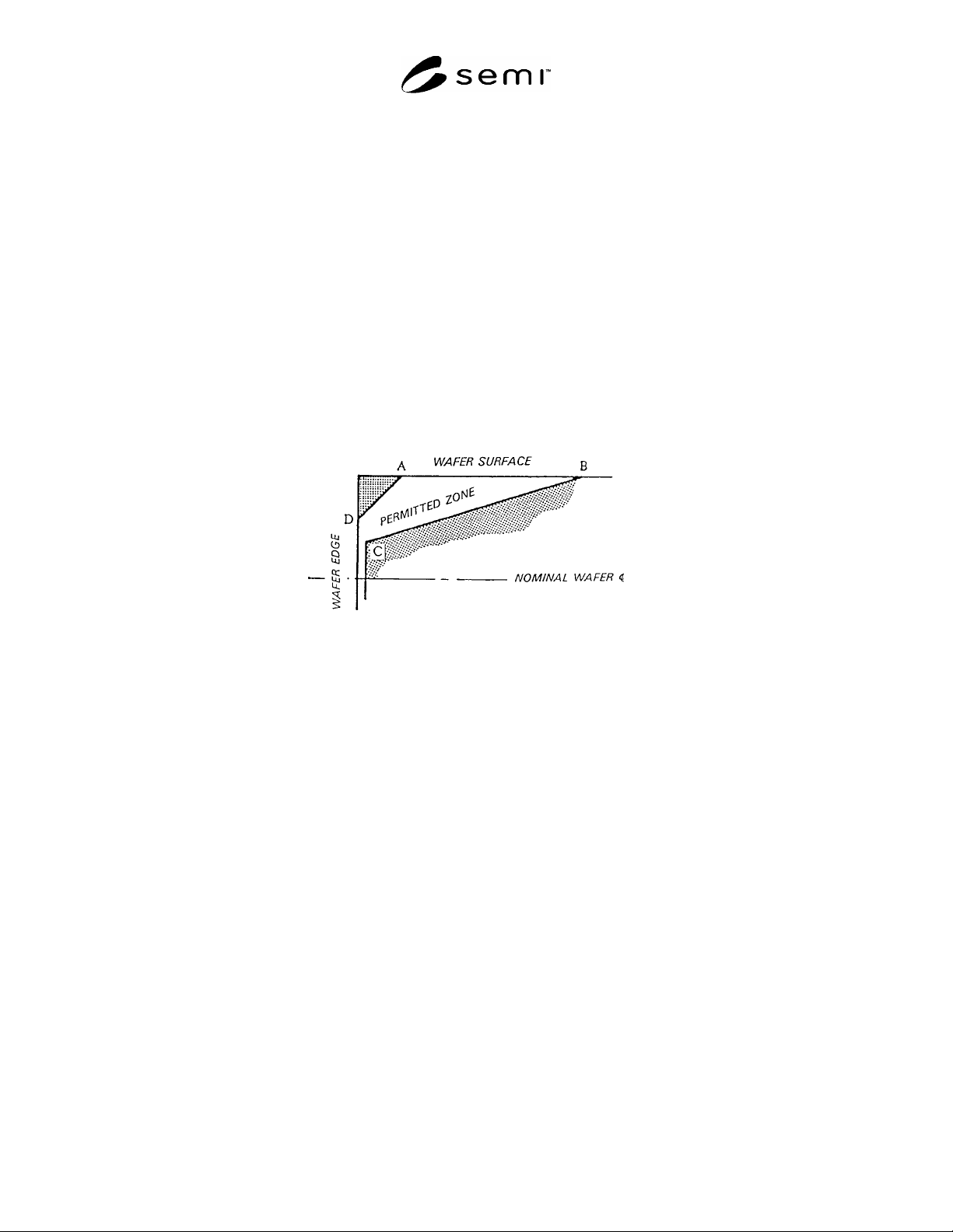
6.4 Template, having transparent regions defining the area through which the contour of the edge of the wafer must
pass and a semi-transparent region bounding the space. An example of a template is given in Figure 1. Instructions
for constructing templates are given in §10.
NOTE: Only half is used to emphasize that these methods are not intended for measurement of thickness.
Figure 1
Template Showing One Half of Wafer Cross Section
6.5 Gage Block or Precision Rod, with dimensions approximately the same as the thickness of the wafer to be
tested and accurately known for use in establishing the magnification of the apparatus.
6.6 Rule, 150 mm (6 in.) long with scale gradations of 0.5 mm (0.02 in.) or less.
7 Sampling
7.1 Unless otherwise specified, ANSI/ASQC Z1.4 shall be used. Inspection levels shall be agreed upon between
the supplier and purchaser.
7.2 The number and location of the test points on the periphery of each wafer shall be agreed upon between the
supplier and purchaser.
8 Specimen Preparation
8.1 For Method A, cleave or fracture the wafer along a diameter.
NOTE 4: This may be conveniently accomplished by positioning the wafer over a small diameter rod and pressing downward on
both sides. Alignment by eye is sufficient. If required by the sampling plan, cleave additional pieces along the edge of the wafer.
9 Determination of Magnification Factor
9.1 For Method A, adjust the comparator or microscope to the magnification to be used for the test. Using a gage
block or precision rod of accurately known dimensions, follow the comparator or microscope manufacturer's
instructions to establish object-to-image magnification to three significant figures.

SEMI MF928-0305 © SEMI 2005 4
9.2 For Method B, position a gage block on the fixture (see ¶6.3) such that the known dimension can be measured
in the vertical direction on the screen using an appropriate rule. Measure the image vertical dimension to the nearest
0.02 in. (0.5 mm) and adjust magnification until the desired magnification for the test is obtained. Reposition the
gage block such that the screen image of the known dimension can be measured in the horizontal direction. Adjust
magnification to give the same value as the vertical.
NOTE 5: Television systems may have distortions in either vertical or horizontal deflection circuits caused by improper settings
of vertical or horizontal size or linearity. If magnification in both horizontal and vertical directions is not equal to the desired
resolution, recalibration of the television system may be required.
10 Preparation of Template
10.1 Multiply each of the chosen or specified template coordinates by the magnification factor.
10.2 Prepare on transparent material a full-scale template having the dimensions calculated in ¶10.1 with a
projected image accuracy of ± 0.5 mm ( 0.020 in.).
10.2.1 Mount the template on the screen such that the images of the wafer surfaces are parallel with the
corresponding template lines. Alternatively, the template can be electronically generated or projected by the optical
system.
11 Procedure
11.1 Method A
11.1.1 Mount the test specimen in the fixture with the cleaved or broken surface of the wafer facing the objective
lens and approximately perpendicular to the viewing direction.
11.1.2 Adjust the comparator focus such that a sharp image of the wafer is seen on the screen.
11.1.3 Position the wafer by appropriate motion of the fixture so that the contour profile image is tangent to the
overlay template at both the edge and front surface.
11.1.4 Determine whether or not the contour of the edge of the wafer between the points of tangency lies entirely
within the permitted zone of the template. If the specification has other requirements, such as those relating to the
specific shape of the profile, inspect the profile image for adherence to such conditions.
11.1.5 Repeat ¶11.1.3 and ¶11.1.4 with the opposite side of the contour profile image tangent to the overlay
template at both the edge and the back surface.
11.1.6 If the test specimen includes the full diameter, reverse the fixture on the comparator table to permit the edge
contour at the opposite end of the wafer diameter to be seen on the screen and repeat ¶11.1.2 through ¶11.1.5.
11.1.7 If additional parts of the wafer were prepared as test specimens, repeat ¶11.1.1 through ¶11.1.5 for each.
11.1.8 Record as “passed” those wafers for which all observed edge contours lie entirely within the permitted zone
and which meet all other specification requirements.
11.2 Method B
11.2.1 Mount a whole wafer in the fixture.
11.2.2 Adjust the focus of the apparatus to give the sharpest image of the extreme edge of the wafer as seen on the
screen.
11.2.3 Position the wafer by appropriate motion of the fixture so that the contour profile image is tangent to the
overlay template at both edge and front surface (see ¶3.1).
11.2.4 Determine whether or not the contour of the edge of the wafer between the points of tangency lies entirely
within the permitted zone of the template. If the specification has other requirements, such as those relating to the
specific shape of the profile, inspect the profile image for adherence to such conditions.
11.2.5 Rotate the wafer in the fixture while continuously observing the contour. Due to diameter and roundness
tolerances, the specimen contour profile image may move with respect to the overlay template while rotating the

SEMI MF928-0305 © SEMI 2005 5
specimen. Adjust wafer or template position and focus as required to assure proper judgment of template fit.
Repeat ¶11.2.3 and ¶11.2.4 at specified points in accordance with the sampling plan.
NOTE 6: Flatted regions of the wafer periphery cannot be evaluated by this test method.
11.2.6 Repeat ¶11.2.3 through ¶11.2.5 with the opposite side of the contour profile image tangent to the overlay
template at both the edge and the back surface.
11.2.7 Record as “passed” those wafers for which all edge contours examined lie entirely within the permitted zone
and which meet all other specification requirements.
12 Report
12.1 Report as a minimum the following information:
12.1.1 Date of test,
12.1.2 Name of person conducting the test,
12.1.3 The lot number of other identification of the material,
12.1.4 Method used, A or B,
12.1.5 Position(s) on the wafer periphery that were examined,
12.1.6 The number of wafers in the lot,
12.1.7 The number of test wafers, and
12.1.8 The number of accepted wafers.
13 Precision and Bias
13.1 Although these test methods do not return a test result, an interlaboratory test was conducted to determine the
reliability of the nondestructive Method B when applied to silicon wafers. In this test, a lot of 25, 125 mm diameter,
edge profiled, silicon wafers was tested in accordance with Method B against the edge contour template and other
requirements of SEMI M1. The wafers were measured by nine different organizations using several types of
commercially available edge contour measuring instruments, all of which had similar optical systems. In one case
the magnification used was 60× instead of 100× as specified in ¶6.2.
13.1.1 In no case was a wafer judged to be within the specification requirements by all participants. Only three
wafers were judged by all participants to fail, but different participants reported different reasons for failure; the
other 22 wafers were judged to pass by some and to fail by others, but again the same failure mode was not always
reported. Most of the difficulty centered around determination of whether or not the edge profile extended further
into the wafer than 0.508 mm (the specified location of point B in the SEMI template). Some participants reported
failure on the front of the wafer, some on the back, and some reported that failure occurred because the contour
passed inside point C. These results confirm the difficulties with locating the wafer surface indicated in ¶3.1. No
participant reported use of the straight-edge technique suggested in ¶3.1, so the efficacy of that procedure was not
evaluated in the test.
13.1.2 The results also confirmed the difficulties with interference from particulate contaminants. Several
observers reported protrusions or sharp points on the wafer periphery, but these were not generally reported.
Examination of the wafers under conditions in which the edge of the wafer could be accessed during the test showed
that such apparent protrusions could be removed by blowing or wiping with lens cleaning tissue.
13.1.3 For more details, refer to the Research Report.
2
13.2 At the recommended magnification, 100×, a dimension of 25 m (0.001 in.) at the object plane produces a
screen image of 2.5 mm (0.1 in.). The smallest size details of edge contours to be inspected by these test methods
are of comparable dimensions.
2 Available on request from SEMI Headquarters, 3081 Zanker Road, San Jose, CA, Telephone 408-943-7021, Fax: 408-943-7015, e-mail:
standards@semi.org. Request International Standards Research Report MF0928.