semi合集-English.pdf - 第6476页
SEMI G78-0699 © SE MI 1999 9 7 Required Hardware Check l i s t (s ee Figur e 7) Wafer prober (if the tes t pla n includes either hot or cold chuck te sting, the p rob er must b e appropriately equipped). A planarized…
SEMI G78-0699 © SEMI 1999 8
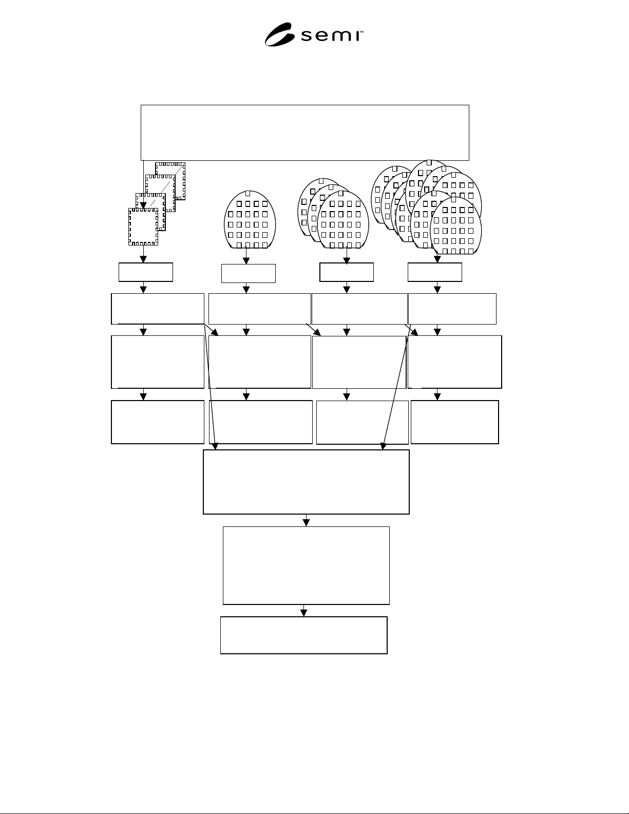
DIE
Normalized Die Offset
(Normalized by Lot)
Average Die Offset - Average Lot Offset
[ACCURACY- TOTAL PROBE SYSTEM ERROR]
Three Sigma Normalized Die Offset
(Normalized by Lot)
Three sigma calculation of
Normalized Die Offset Value
[REPEATABILITY]
Three Sigma Total Probe System Error Range
Average Lot Offset +/- Total Probe System Error
VISION SYSTEM or PROBE MARK ANALYSIS SYSTEM
ESTABLISH
PAD OFFSETS
Offset from the center of the bond pad to the center of the scrub mark for all pads analyzed
Average Die Offset
Average all Pad Offsets by
die
Normalized Pad Offset
(Normalized by Die)
Pad Offset – Avg. Die
Offset
Three Sigma Normalized
Pad Offset
(Normalized by Die)
Average Wafer Offset
Avg. of Avg. Die Offset
Three Sigma Normalized
Die Offset
(Normalized by Wafer)
Normalized Die Offset
(Normalized by Wafer)
Avg. Die Offset – Avg. Wafer
Offset
Normalized Wafer Offset
(Normalized by Setup)
Avg. Wafer Offset – Avg.
Setup Offset
Three Sigma Normalized
Wafer Offset
(Normalized by Setup)
Normalized Setup Offset
(Normalized by Lot)
Avg. Setup Offset – Avg.
Lot Offset
Three Sigma Normalized
Setup Offset
(Normalized by Lot)
SETUP LOT
WAFER
1
2
Average Setup Offset
Avg. of Avg. Wafer Offset
7
3
8
4
5
6
9
Average Lot Offset
Avg. of Avg. Setup Offset
10
11
12
13
15
14
Figure 6
Pad Offsets and 15-Step Analysis Algorithm for Determining Probe System Error
SEMI G78-0699 © SEMI 19999
7 Required Hardware Check list (see Figure 7)
Wafer prober (if the test plan includes either hot or
cold chuck testing, the prober must be
appropriately equipped).
A planarized and aligned probe card which
matches the selected wafers, accompanied by a
metrology tool printout of the ‘x’, ‘y’ and ‘z’
positions of all of the probe tips to be used for
probe mark analysis. Note: The probe card should
be measured for alignment, but not ”tweaked”,
immediately prior to and after the conclusion of
each subsequent test.
Untested wafers
A special “test program” with a fixed “test” time.
Tester or PC that will run the “test program”. If a
PC is used to simulate the tester, it must be
equipped with the appropriate hardware for
communication with the wafer prober.
A stopwatch, with 0.1 second resolution. The
stopwatch is to have “split” capability.
Note that the user of this method may choose at
their discretion to utilize any other time stamp
logging technology at their disposal, so long as the
computational overhead of this logging has no
effect upon the throughput of the prober.
8 Requirements (see Figure 7)
8.1 Qualified Prober — Before initiating the test
process, the wafer prober is to be certified by a
representative of the prober manufacturer to be fully
operational.
8.2 Qualified Personnel — The individual running the
wafer prober for the test procedure must be certified or
otherwise qualified to operate the prober being tested.
9 Test conditions (see Figu re 7)
9.1 Test Time — a fixed “device te st time” will be
used during these tests. The recommended value for
this test time is 1.0 seconds.
9.2 Accuracy and Repeatability vs. Throughput — The
person or manufacturer running this test may make a
choice (or choices) as to how they elect to balance
accuracy and repeatability with throughput, but all three
tests must be run simultaneously. This will generate a
set of numbers defining a particular prober's accuracy
and repeatability at a given throughput (or a throughput
at a given accuracy and repeatability). All adjustments
to the prober are to be made using standard, end-user-
adjustable settings, and all prober settings associated
with a particular throughput / accuracy and repeatability
combination are to be included in the final report.
9.3 Temperature — This test can b e conducted at any
temperature, however, numerous variable can distort
the results if run at a temperature other than ambient,
i.e. probe tip drift due to an increase or decrease in
temperature.
• Cautionary Note: If the tests are performed at
temperatures other than ambient, the user must use
the same probe card and wafer type for all tests
across all test platforms to ensure uniformity of
results.
9.4 Probe Card Type — All types of probe cards
(blade, peripheral / cantilever or vertical) may be used,
so long as they leave a visible scrub mark.
• Cautionary note: Some vertical probe cards exhibit
an inherent amount of ‘x’ - ‘y’ needle drift. The
user should verify the intrinsic repeatability of the
probe card before using it to characterize the
prober.
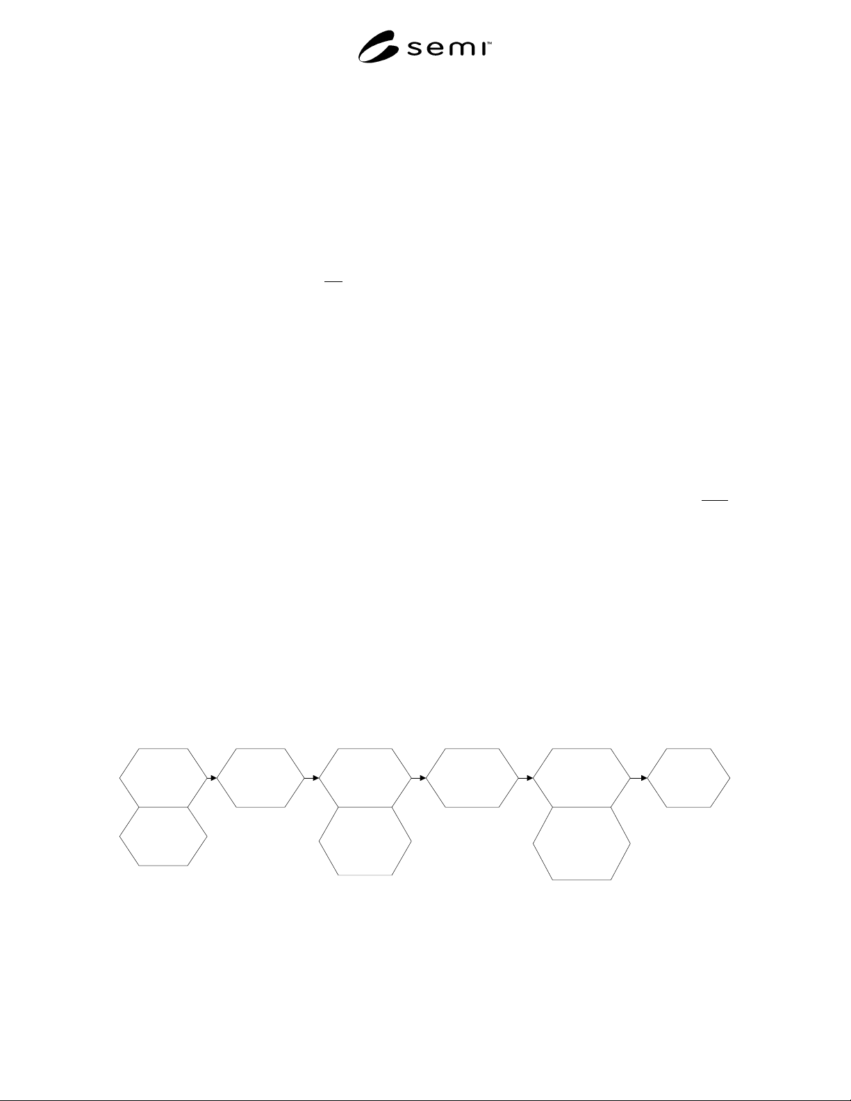
Prober
available?
Probe card
available?
"Test
Program"
available?
Stop-
watch
available?
Is Prober
"Qualified"?
Condition of
probe card
known,
documented?
Personnel
"Qualified"?
Hardware to
run "Test
Program"
available and
tested?
Untested
wafers
available?
7.0 8.2 7.0
9.5
7.0 7.0
7.0
7.0
8.1
Figure 7
Preparation
SEMI G78-0699 © SEMI 1999 10
9.5 Probe Card Condition — a me trology tool
printout verifying the ‘x’, ‘y’ and ‘z’ position of each
probe is within the users specification must accompany
the probe card.
9.6 Tester – Prober Communications — The type of
communications method used between the prober and
the tester is left up to the user of this test method.
Because communication overhead varies with protocol,
the same hardware and “test program” (modified as
necessary to communicate to the prober under test)
must be used for all tests.
9.7 Presence of the PTI — During the test, the probe
card must have loading similar to that applied by the
normal “in use” application such as a Probe Test
Interface (PTI) or Direct Docking Pogo Stack. The
force exerted on the probe card by the PTI will stabilize
the probe card, improving the repeatability of the data
collected.
9.8 Wafer Cassette — For the purp oses of these tests,
a cassette of wafers is defined as containing ten wafers.
Ensure the wafers are placed in the same slots for each
test.
10 Test Procedure (see Figur es 8 and 9)
10.1 Load wafer cassette
10.2 Install probe card
10.3 Set probe mode to serpentine, set all other
necessary prober parameters. N
OTE THAT ALL DIE ON
ALL WAFERS ARE TO BE “TESTED”, NOT JUST THE 12 DIE
FROM WHICH PROBE MARK DATA WILL BE ANALYZED.
10.4 Note all applicable parameters (see chart below)
10.5 If temperature testing, soak for a user-defined
time (consistent with the user’s test methodologies) that
is equal on all corresponding tests on all probers being
evaluated.
10.6 Start probing process and stop watch
simultaneously.
10.7 The “test program” must perform automatic
alignment of the probe card to the wafer prior to wafer
#’s 1, 2, 5, and 8.
NOTE: While not required, it is recommended that the PTI
and Probe Card be removed and re-installed prior to each of
the automatic alignment steps to simulate whatever locational
error might be induced by manipulation of the interface and
the probe card.
10.8 Record times of individual eve nts (utilizing the
stopwatch’s “split” function) on the supplied chart or a
similar form.
10.9 When the last wafer is finished and has been
returned to wafer cassette, stop the stopwatch.
10.10 Collect the probe mark offset data from wafers.
10.11 Calculate Normalized (by lot) Die Offset
[Accuracy] and 3σ of Normalized (by lot) Die Offset
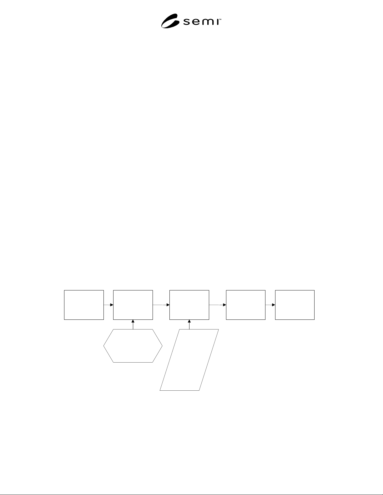
[Repeatability]:
Place boat of
wafers in wafe
r
handler
Install probe card
If test environment
is "overhead",
install PTI and/or
dock test head
Set up prober for
test
This
procedure
will var
y
depending
upon the
prober type
being used,
the wafer
layout, and
many other
variables.
Document all
prober settings
If testing at other
than ambient
temperature, pre-
soak
10.1 10.2
10.7
10.3 10.4 10.5
Figure 8
Setup