semi合集-English.pdf - 第7529页
SEMI MF1771-0304 © SEMI 2003, 2004 6 5. Divide the curre nt value measured at the previous point by the capacitor area , and record this value a s the hard failure current de nsity. 9.10 Afte r hard failure has been det …
SEMI MF1771-0304 © SEMI 2003, 2004 5
7.2 Shielded Triaxial Cables — Involving guarding to
minimize the noise when measuring low current values.
7.3 Wafer Chuck — Electrically isolated from its
case/probe platen. While the chuck may be connected
to the reference voltage (zero, not ground), lower
electrical noise may be obtained by connecting the
voltage ramp source to the chuck and measuring the
current through the probe connection.
7.4 Probe — To contact the gate electrode. Either a
hard needle-type probe such as tungsen carbide (which
may be a single probe or a probe card) or a mercury
probe may be used.
8 Sampling
8.1 Sampling is the responsibility of the user of this
test method. However, if testing is done as part of a
comparison or correlation, sampling shall be agreed
upon in advance by all participants.
NOTE 2: Refer to the appendix of Standard 35 for a good
discussion of sampling plan statistics.
9 Procedure
9.1 Before the measurement, record the following
information for each sample: sample identity, date,
time, operator, instrument station identity (if any),
average oxide thickness, gate area in square
centimeters, gate material, oxide type (example thermal
versus deposited), structure type, conductivity type (n
or p), bias mode (accumulation or depletion), test
temperature.
9.2 Establish the test parameters relevant to the test
system and the sample. These include the voltage ramp
rate, computed in accordance with the calculation in
Section 10.2, and the noise threshold level and in some
instances the ln J-V slope ratio for the hard failure
criterion in Section 9.9.5, both determined in
accordance with the calculation in Section 10.3.
9.3 Set the applied voltage to zero volts.
9.4 Recognizing that some information on extrinsic
defects may be lost, perform a pretest as follows. If it is
desired not to lose the information on extrinsic defects,
proceed to Section 9.5.
9.4.1 Bias the gate into accumulation at the voltage of
use. If the measured current exceeds a value equivalent
to 1.0 × 10
–5
A/cm
2
(or a current value of 10 nA if the
device area is at or below 10
–3
cm
2
), record this device
as a Category 0 failure and proceed to Section 9.11.
9.5 From the starting bias condition (zero if no pretest
was done, or the voltage of use if a pretest was used)
record voltage and current.
9.6 Begin increasing the voltage bias at a rate
equivalent to an electric field increment of 1.0 ± 0.1
MV-cm
–1
-s
–1
. Note that other ramp rates may be used
if it can be shown that it does not affect the results, or if
it is agreed upon by all parties to the test.
9.7 Record current-voltage data at an interval no more
than 0.1 s between readings, or at least once near the
end of each voltage step.
9.8 After each current reading, test to see if any of the
soft failure criteria have been met. If so, store the
appropriate value.
9.9 After each current reading, check to see if one of
the hard failure criteria has been reached.
9.9.1 Check to see if the current has increased to a
value greater than or equal to 0.98 times the compliance
limit of the voltage ramp source. If so, record the
previous voltage level as the hard failure voltage, and
set the failure category to 1. Divide the current level at
the previous measurement point by the capacitor area,
and record this value as the hard failure current density
for this unit.
9.9.2 Check to see if the current has increased by a
factor of 1000 or more from the previous reading. If so,
record the previous voltage level as the hard failure
voltage, and set the failure category to 2. Divide the
current value measured at the previous point by the
capacitor area, and record this value as the hard failure
current density.
9.9.3 Check to see if the current has increased by a
factor of 10 or more in two consecutive voltage steps.
If so, record the previous voltage level as the hard
failure voltage, and set the failure category to 3. Divide
the current value measured at the previous point by the
capacitor area, and record this value as the hard failure
current density.
9.9.4 If the current is above the noise threshold level,
check for an abrupt increase in the current by a factor of
ten. If this has occurred, record the previous voltage
level as the hard failure voltage, and set the failure
category to 4. Divide the current value measured at the
previous point by the capacitor area, and record this
value as the hard failure current density.
9.9.5 If the current is above the noise threshold level,
check for an abrupt change in the logarithmic slope of
the current density-voltage characteristic of the unit.
To minimize the chance of detecting a false reading,
use the average of the previous five (V,I) data pairs to
compute the established slope, and the current and
previous (V, I) data pairs to compute the new slope. A
change by a factor of three shall constitute a failure. If
this has occurred, record the previous voltage level as
the hard failure voltage, and set the failure category to
SEMI MF1771-0304 © SEMI 2003, 2004 6
5. Divide the current value measured at the previous
point by the capacitor area, and record this value as the
hard failure current density.
9.10 After hard failure has been detected by one of the
criteria in Section 9.9 or the upper test voltage limit has
been reached, perform a post-test using the same
criteria defined for the pretest in Section 9.4.1. This is
to be done whether a pretest was elected in Section 9.4
or not. If the unit fails the post-test conditions, modify
the failure category in some way to reflect this
observation. For example, one may change the sign of
the failure category number, or add an asterisk.
9.11 Proceed to the next device to be tested, and repeat
Sections 9.3–9.10 until all devices are tested.
10 Calculations
10.1 Current and Current Density — To calculate
current (I) from a current density (J), multiply the
current density by the area of gate contact (A) as
follows:
AJI ×= (1)
NOTE 3: Example: Given a current density (J) of 1 µA/cm
2
and a gate area (A) of 0.08 cm
2
, the current would be 80 nA.
10.1.1 Similarly, compute current density (J in A/cm
2
)
from measured current (I in A) and area (A in cm
2
)
using
A
I
J = (2)
10.2 Oxide Voltage and Electric Field Strength as a
Function of Applied Voltage — Since ramp voltage test
increments and ramp rates as well as some breakdown
voltage data analyses are specified in terms of oxide
electric field strength, it is important to consider the
conversion of applied voltages to oxide voltage and
electric field values for these two cases. Historically,
oxide electric field strength has been approximated
simply by dividing the applied voltage by the thickness
of the oxide. This approximation is in error because it
neglects the offset in the zero values of applied and
oxide voltage brought about by the work function
difference between gate electrode and silicon substrate,
and the voltages dropped across the substrate (and the
gate electrode, if it is non-metallic) when the capacitor
is strongly biased during breakdown testing. These
voltage drops are made up of two components; one
associated with band bending at the interfaces with the
oxide that establishes the high fields required for
testing, and another involving additional voltage drops
due to series resistances that become significant at very
high currents. These corrections, which together
normally range up to 1 to 2 V in magnitude, might
reasonably be neglected for samples with oxides greater
than 20-nm thick, as the correction amounted to only a
few percent of the breakdown voltage values. For
thinner oxides, these additional voltage components
must be taken into account.
10.2.1 The voltage V
app
applied across an MOS
capacitor with a given gate-substrate work function
difference Φ
ms
and oxide fixed charge Q
f
may be
expressed as follows:
gatesubms
ox
f
oxapp
VV
C
Q
VV ++
Φ+−= (3)
where:
V
ox
= voltage across the oxide, V,
C
ox
= oxide capacitance, F/cm
2
,
V
sub
= voltage across the substrate, V,
V
gate
= voltage across the gate electrode (arising
from polysilicon depletion or series
resistance, V.
10.2.2 At zero volts applied, the offset due to the work
function difference and oxide charge appears
predominantly across the oxide. For setting a voltage
ramp rate, the incremental change in V
ox
with changing
V
app
is not affected by this offset, but may be decreased
by voltage increases across the silicon substrate or the
gate electrode due to band bending and series resistance
drops. For a sample in which the applied bias voltage
polarity accumulates the substrate, and the gate
electrode is metallic or of the opposite conductivity
type from the substrate (for example, p-type silicon
substrate and n+ polysilicon gate), these effects are
appreciable only for very small and very large applied
voltages. At low bias, silicon bands bend until the
surface becomes degenerate, after which the rate of
band bending becomes very low. At high biases,
significant resistive voltage drops may develop if the
test structure design is not optimized. Over the largest
portion of the test in which neither of these effects are
large, ramp rates may be computed assuming that
voltage increments applied to the device under test
appear completely across the oxide, and ∆E
ox
, the
electric field increment across the oxide, is given as
follows:
ox
app
ox
W
V
E
∆
=∆ (4)
where:
W
ox
= oxide thickness, cm.
10.2.3 For computations of oxide field strength
associated with the various hard and soft failure criteria,
SEMI MF1771-0304 © SEMI 2003, 2004 7
all corrections indicated in Equation 3 must be taken
into account.
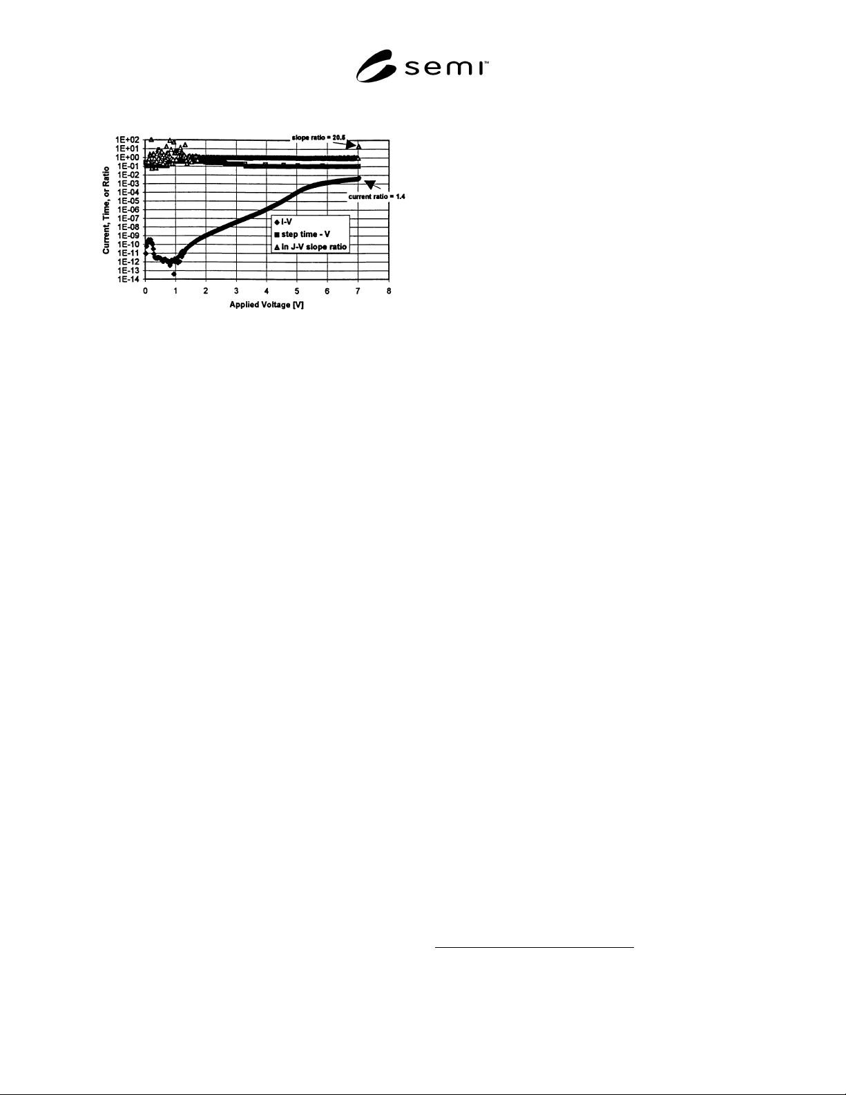
Figure 2
Determination of Noise Threshold Current Level,
Slope Ratio Applicability, and Voltage Step Time
Variations
10.3 Determination of Noise Threshold Current Level
and ln J-V Slope Ratio Specification — Useable values
of noise threshold current level and ln J-V slope ratio
depend upon properties of the test system as well as the
samples to be evaluated, and a preliminary test may be
required in order to specify them properly. To do this,
it is necessary to store all the current-voltage data pairs
as well as the incremental voltage step time readings in
data arrays. This is not required for performance of the
bulk of the testing, but is sometimes useful for more
thorough analysis of the test results. When such data is
stored, it is possible to construct a figure like that
shown in Figure 2, which is a semi-logarithmic plot of
sample current, step time, and slope ratio versus applied
voltage. Data given here was taken on a 3-nm oxide on
a p-type silicon substrate, so the current and voltage
values are magnitudes of negative readings. Both direct
and Fowler-Nordheim tunneling components are seen
in the I-V data.
10.3.1 To determine the noise threshold current level,
examine the ln J-V slope ratio, shown as open triangles
in Figure 2. It is seen to be quite noisy for this test
system and sample up to a current level just below 1
nA. This value, 1 nA, is thus a good choice for noise
threshold current level for this test. Further analysis of
the slope ratio data shows that its maximum value in the
range from 1 nA up to catastrophic failure is 1.21, so
the standard specified ratio value of three (3) is
adequate to avoid significant noise interference.
10.3.2 The step time-voltage dependence plotted as
light squares in Figure 2 illustrates shortcomings in the
step time control for this configuration of the
measurement system. A voltage step time of 0.1 s is
specified for this test method in Sections 5.3 and 9.7.
Because of the high, time-dependent currents measured
below 0.5 V, there is a regime below 1 V where this is
observed, but most readings from there up to a current
value of 0.1 µA fall in the range 0.2 to 0.4 s. Also, for
higher current values, there are singular points at
electrometer range changes where 0.2-s delays are
encountered. It has been shown (Klema
4
) that
deviations of this amount do not have large effects on
breakdown voltage distributions, but these extended
delays affect total measurement time, and it would be
worthwhile to eliminate them if possible. Approaches
depend upon measurement hardware being used, but
trading off low current resolution for electrometer
autoranging time and look-ahead range changing code
are possibilities.
10.4 ln J-V Slope Hard Failure Criterion — Hard
breakdown failure of oxides is increasingly difficult to
detect as oxide thickness decreases below 10 nm.
Fowler-Nordheim emission, the dominant current
transport mechanism for SiO
2
films in this thickness
range, predicts that at a given field strength, the
logarithmic slope of the J-V characteristic increases for
decreasing film thickness, but decreases with increasing
field strength for a given oxide thickness. Thus, a
change in ln J-V slope may be a more sensitive detector
of failure for these very thin films, where high failure
current density, low oxide impedance at failure, and
high voltage drops in series resistances might lead to
very small current changes when the oxide ruptures.
10.4.1 Experience with this failure criterion for oxide
thicknesses ranging down to 3 nm indicates that a
change by a factor of 3 provides good detection of
failure while remaining above the noise level in the
data. Users may verify this condition for their
particular sample and test conditions, and change the
failure factor accordingly. Any such change must be
agreed upon by the parties to the test, and clearly
identified in the report of the data.
10.4.2 In order to minimize noise in the calculated
values and optimize the sensitivity of the failure
detection, it has been found advisable to use a set of
five data points to calculate the established and new
values of the ln J-V slope. This illustrated in Figure 3,
which shows the last few data points in the ramp
voltage test of a 50-nm oxide. Data points are spaced at
0.1 MV/cm increments, as dictated by this test method.
10.4.3 In particular, the last five data points are labeled
(V(n), I(n)) through (V(n – 5), I(n – 5), respectively.
The established logarithmic slope is as follows:
4 Klema, J., “Ramp Rate Effect on Dielectric Breakdown,” Final
Report, IEEE International Integrated Reliability Workshop (IRW),
IEEE Electron Devices Society, 1989, p. 87.