semi合集-English.pdf - 第5300页
SEMI M48-1101 © SEMI 2001 10 -100 -8 0 -6 0 -4 0 -2 0 0 20 40 60 80 100 - 100 -80 -60 - 40 - 20 0 20 40 60 80 100 Figure 7 Spiral Scan Example - 200 mm Di ameter Wafer, 81 Points NOTICE: SEMI makes no warranties or repre…
SEMI M48-1101 © SEMI 2001 9
R
nominal
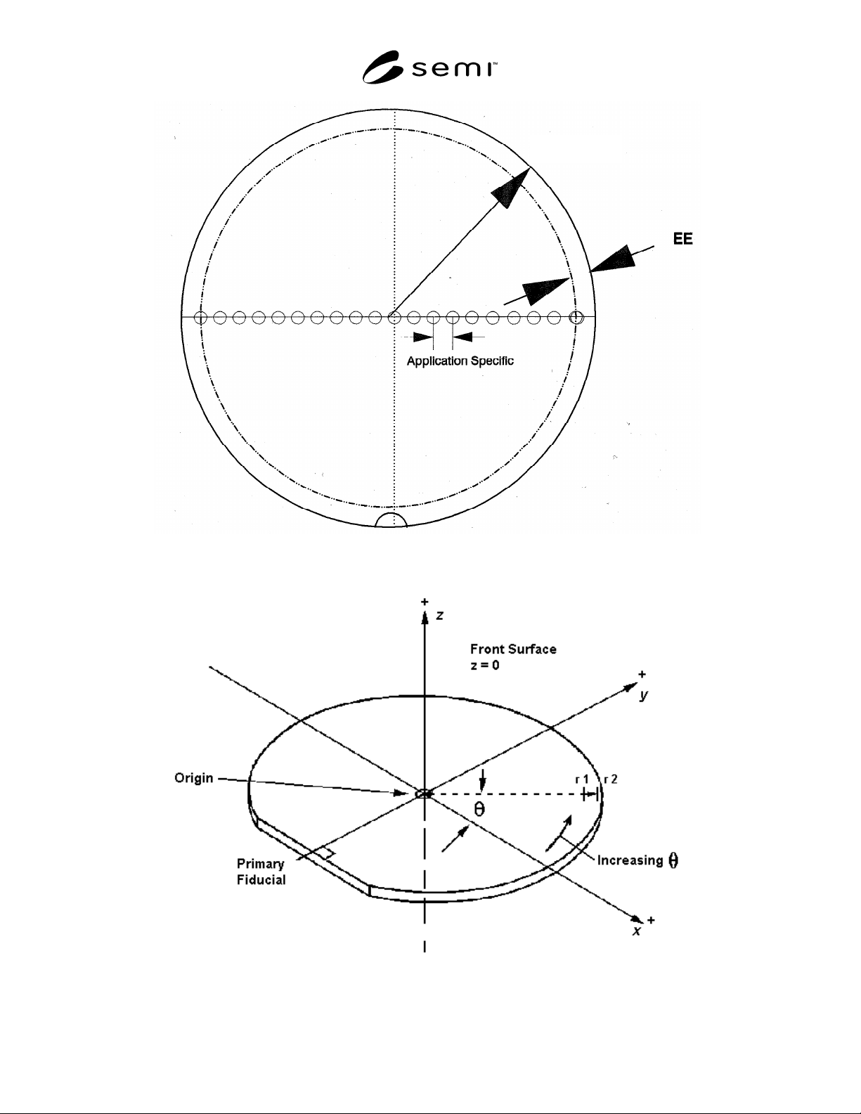
Figure 5
Single-Diameter High-Density Measurement Sites
Figure 6
Edge Scan Location
SEMI M48-1101 © SEMI 2001 10
-100
-80
-60
-40
-20
0
20
40
60
80
100
-100 -80 -60 -40 -20 0 20 40 60 80 100
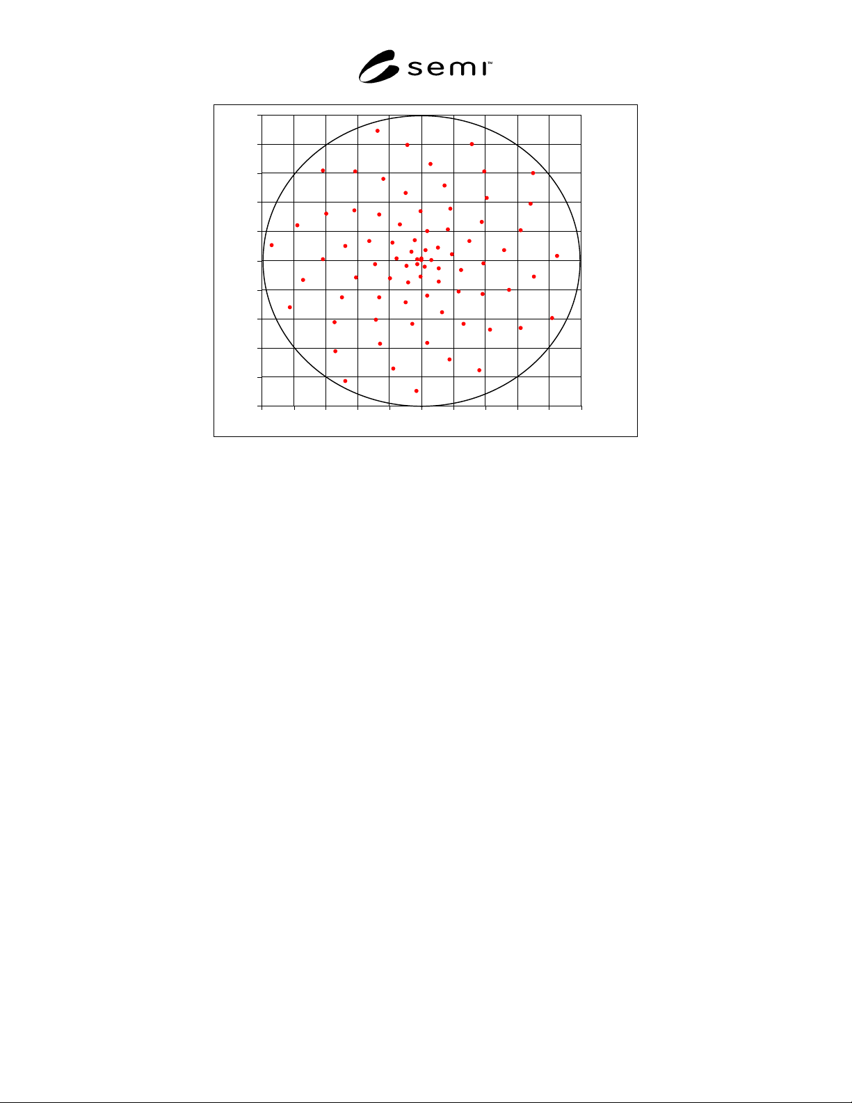
Figure 7
Spiral Scan Example - 200 mm Diameter Wafer, 81 Points
NOTICE: SEMI makes no warranties or representations as to the suitability of the standards set forth herein for any
particular application. The determination of the suitability of the standard is solely the responsibility of the user.
Users are cautioned to refer to manufacturer's instructions, product labels, product data sheets, and other relevant
literature, respecting any materials or equipment mentioned herein. These standards are subject to change without
notice.
By publication of this standard, Semiconductor Equipment and Materials International (SEMI) takes no position
respecting the validity of any patent rights or copyrights asserted in connection with any items mentioned in this
standard. Users of this standard are expressly advised that determination of any such patent rights or copyrights, and
the risk of infringement of such rights are entirely their own responsibility.
SEMI M48-1101 © SEMI 2001 11
RELATED INFORMATION 1
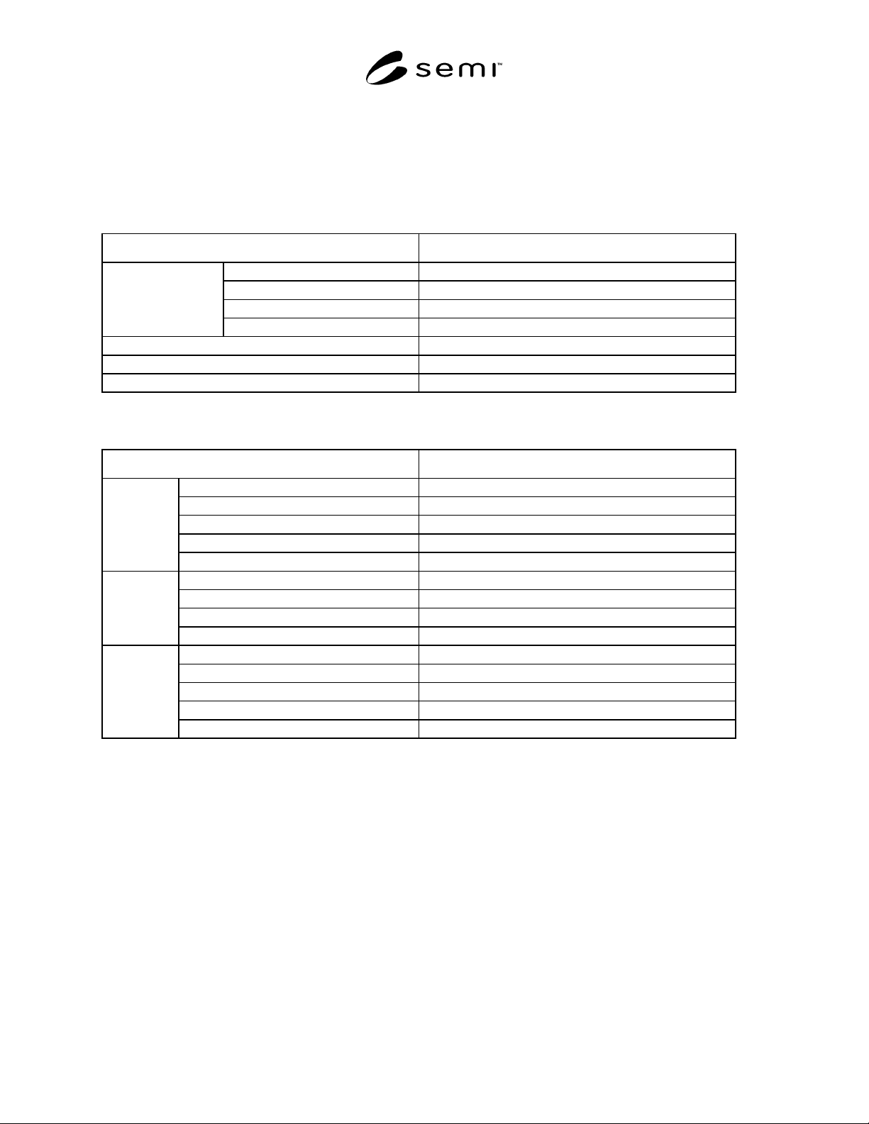
CMP PROCESS TEST GUIDE
NOTE: This related information is not an official part of SEMI M48, and is not intended to modify or supercede the
proposed standard. It is provided for information purposes.
Table R1-1 Recommended Values for Wafer and Insulating Film Thickness for CMP Process Test
Item Guideline
Bow –25 µm to +25 µm
Warp ≤ 25 µm
GBIR (previously called TTV) ≤ 4 µm
Wafer
(See NOTE 1.)
SBIR (20 × 20 mm site) ≤ 0.5 µm
Starting Insulating Film Thickness 1000 – 1500 nm
Starting % WIWNU ≤ 2% of mean thickness
Final Insulating Film Thickness 50% of starting film thickness
NOTE 1: See SEMI M1 for definitions of listed wafer parameters.
Table R1-2 Recommended Values for Wafer and Metal Film Thickness for CMP Process Test
Item Guideline
Bow –25 µm to +25 µm
Warp ≤ 25 µm
GBIR (previously called TTV) ≤ 4 µm
SBIR (20 × 20 mm site) ≤ 0.5 µm
Wafer
(See
NOTE 1.)
Insulating Film Thickness ≤ 600–1000 nm
Starting TiN Film Thickness 25–30 nm
Starting W Film Thickness 800 nm
Final W Thickness 50% of starting W film thickness
W Stack
W Stack % WIWNU ≤ 2% of mean thickness
Starting Glue Layer (Ta or TaN) Thickness 20–50 nm
Starting Cu Seed Layer Thickness 100–150 nm
Plated Cu Film Thickness As required by application
Final Cu Film Thickness 50% of plated Cu film thickness
Cu Stack
Cu Stack % WIWNU ≤ 8% of mean thickness
NOTE 1: See SEMI M1 for definitions of listed wafer parameters.
NOTICE: SEMI makes no warranties or representations as to the suitability of the standards set forth herein for any
particular application. The determination of the suitability of the standard is solely the responsibility of the user.
Users are cautioned to refer to manufacture's instructions, product labels, product data sheets, and other relevant
literature, respecting any materials or equipment mentioned herein. These standards are subject to change without
notice.
By publications of this standard, Semiconductor Equipment and Materials International (SEMI) takes no position
respecting the validity of any patent rights or copyrights asserted in connection with any items mentioned in this
standard. Users of this standard are expressly advised that determination of any such patent rights or copyrights, and
the risk of infringement of such rights are entirely their own responsibility.
Copyright by SEMI® (Semiconductor Equipment and Materials
International), 3081 Zanker Road, San Jose, CA 95134. Reproduction o
f
the contents in whole or in part is forbidden without express written
consent of SEMI.