semi合集-English.pdf - 第6151页
SEMI G31-0997 © SE MI 1986, 1997 5 Figure 5 Orifice Figure 6 Cover NOTICE: T hese st andards do n ot purport to address safety issu es, if any, associated with their use. It is t he responsibility of the user o f th e se…
SEMI G31-0997 © SEMI 1986, 1997 4
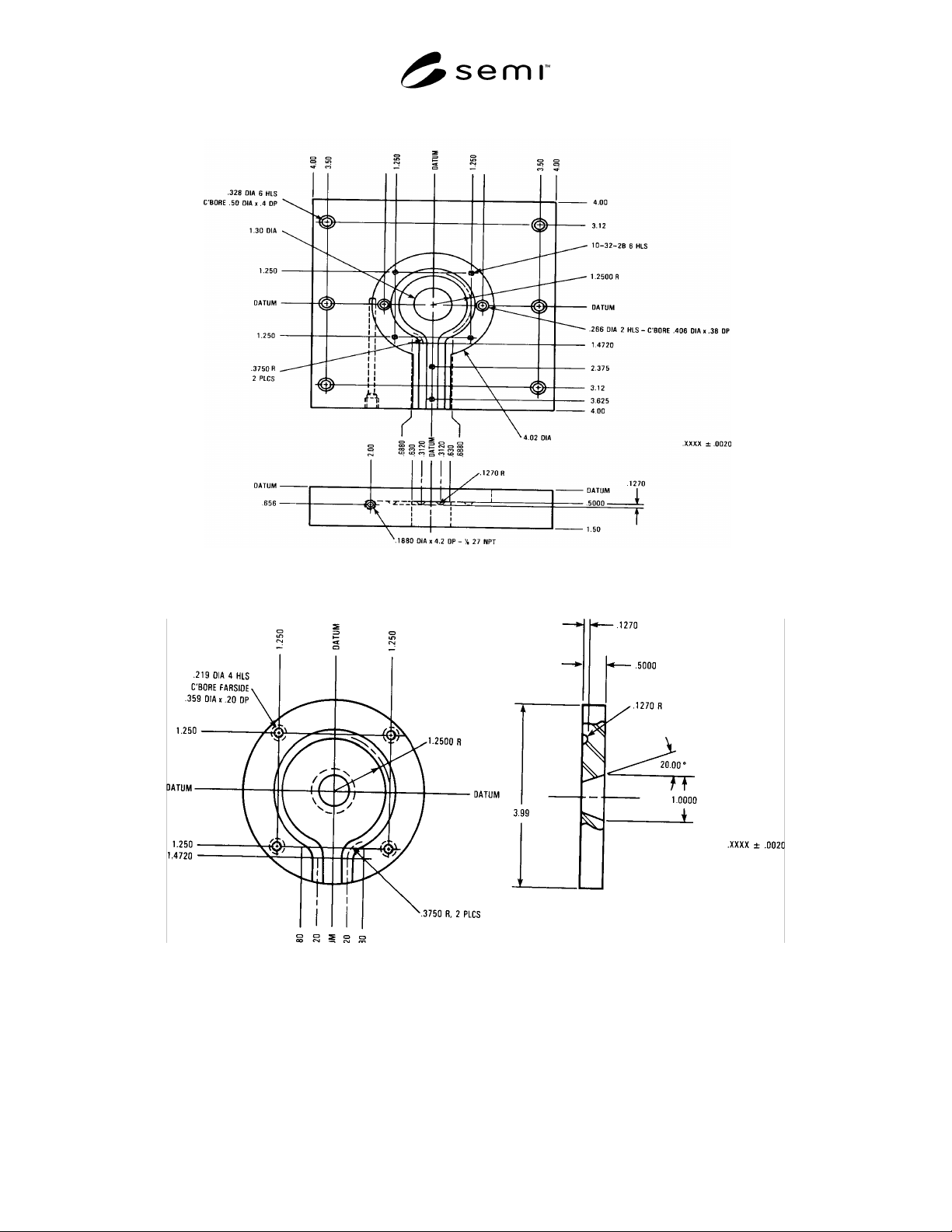
Figure 3
Top Plate
Figure 4
Orifice Holder
SEMI G31-0997 © SEMI 1986, 19975
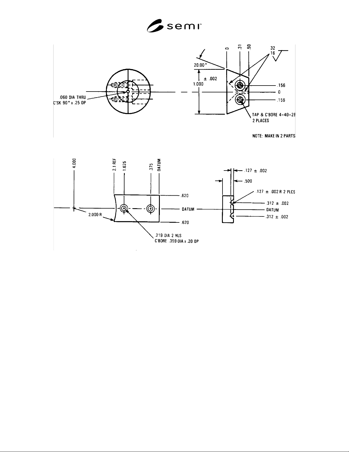
Figure 5
Orifice
Figure 6
Cover
NOTICE: These standards do not purport to address safety issues, if any, associated with their use. It is the
responsibility of the user of these standards to establish appropriate safety and health practices and determine the
applicability of regulatory limitations prior to use. SEMI makes no warranties or representations as to the suitability
of the standards set forth herein for any particular application. The determination of the suitability of the standard is
solely the responsibility of the user. Users are cautioned to refer to manufacturer’s instructions, product labels,
product data sheets, and other relevant literature respecting any materials mentioned herein. These standards are
subject to change without notice.
The user’s attention is called to the possibility that compliance with this standard may require use of copyrighted
material or of an invention covered by patent rights. By publication of this standard, SEMI takes no position
respecting the validity of any patent rights or copyrights asserted in connection with any item mentioned in this
standard. Users of this standard are expressly advised that determination of any such patent rights or copyrights, and
the risk of infringement of such rights, are entirely their own responsibility.
Copyright by SEMI® (Semiconductor Equipment and Materials
International), 3081 Zanker Road, San Jose, CA 95134. Reproduction o
f
the contents in whole or in part is forbidden without express written
consent of SEMI.

SEMI G32-94 © SEMI 1986, 19941
SEMI G32-94
GUIDELINE FOR UNENCAPSULATED THERMAL TEST CHIP
1 Preface
This guideline details recommendations for a
standardized thermal test chip design for referee test
purposes. A sample data format for the test chip can be
found in Appendix A. Based on the results of computer
simulations of various chip-substrate configurations
(Section 3.1), the following recommendations are made
for the design of thermal test chips for VLSI package
characterization (Section 3.2).
2 General Guideline
2.1 Heat Sources — The heat sources (i.e., transistors
or resistor stripes), should use as much of the active
chip area as possible so that the measured package
thermal resistance is indicative of the chip size being
used. A 10 mil (0.25 mm) parameter stripe (inactive
area) should be sufficient for bonding pads and scribe
lanes. It is desirable to use a range of test chip sizes so
that the package thermal resistance can be determined
as a function of chip size. A basic cell size of 75 mil
(1.91 mm) square with a power dissipation capability of
7.5 to 10 W is recommended. The heat source area
should exceed 85% of this basic cell active chip area.
This basic cell could be arrayed or scaled up to a 450
mil (11.43 mm) square chip in increments of 75 mil
(1.91 mm) on a side. For larger chip sizes, the basic cell
size should be chosen so arrays can match the chip sizes
in actual use. Since the larger chips can be 15—20 mm
per side, the basic cell may need to be 5 mm per side,
so a 3 × 3 array can be 15 mm square minimum.
2.2 Spacing between Heat Sources — The spacing
between heat sources, which is needed to accommodate
the temperature-sensing elements (i.e., p-n junctions),
should be minimized. The spacing should be less than
or equal to 2 mil (0.051 mm). The sensing element
should be located at the center of the chip surface. For
chips that are built up from an array of standard cells,
sensing elements are also needed near a corner and
between two adjacent corners (i.e., near or in the
inactive regions), of the basic cell. Additional sensing
elements for such purposes as die attachment evaluation
and non-uniform power dissipation studies may be
included as appropriate. All sensing elements and
associated metallization runs must be electrically
isolated from the heat sources.
2.3 Thermal Test Chip Thickness — The thermal test
chip thickness should be between 18 mil (0.46 mm) and
22 mil (0.56 mm). For thin packages, the test chip
thickness should be reduced to the normal die thickness
for that package.
2.4 Thermal Test Chip — The ther mal test chip should
be designed such that its power dissipation limitations
are consistent with the range of package thermal
resistance encountered. This includes properly designed
metallization runs such that for arrayed test chips,
heating current for inner chips is routed so that wire
runs from the package to inner chips are minimized.
The ability to cause a chip surface-to-case temperature
difference of at least 20°C is desirable. To accomplish
this for silicon chips mounted on a variety of substrates
(ranging from alumina to beryllia), the basic cell
structure (i.e., 75 mil (1.91 mm) on a side) should
dissipate a minimum of 7.5 W.
2.5 Bond Pads — Band pads (clear opening) should be
equal to or greater than 4 mil (0.10 mm) on a side.
Sensing and heating elements should not be connected
to common bonding pads. Bonding pad location and
size can or should be configured such that for arrayed
test chips, chip-to-chip bonding is facilitated (i.e.,
bonding wire runs from the package to inner chips are
minimized), but this is not mandatory for acceptable
functional operation.
2.6 Temperature-Sensing Diode/Diode Bridge
Elements — The temperature-sensing diode/diode
bridge elements should be usable over the complete
operating power and temperature range of the thermal
test chip. The thermal test chip should function at
junction temperature of 130°C minimum.
2.7 Arrayed and Scaled Up Thermal Test Chips —
Pictorial representation of arrayed and scaled up
thermal test chips are depicted in Figures 1 and 2,
respectively. Heating elements (shaded areas) are
transistors or resistor stripes connected in a variety of
series-parallel combinations on as well as off the chip.
The heating elements should fill as much of the shaded
area as practical (consistent with the integrated circuit
layout design rules).
3 References
3.1 Albers, J., “Semiconductor Measurement
Technology: TXYZ: A Program for Semiconductor IC
Thermal Analysis,” NIST Spec. Publ. 400-76 (April
1984).
3.2 Oettinger, F.F., “Thermal Evaluation of VLSI
Packages Using Test Chips — A Critical Review,”
Solid State Technology 27, 169 - 179 (Feb. 1984).