semi合集-English.pdf - 第5323页
SEMI M51-0303 © SEMI 2002, 2003 1 SEMI M51-0303 TEST METHOD FOR CHARACTERIZING SILICON WAFERS BY GATE OXIDE INTEGRITY This test method was technically approved by th e Global Silicon Wafer Committee and is the direct res…
SEMI M50-1104 © SEMI 2001, 2004 8
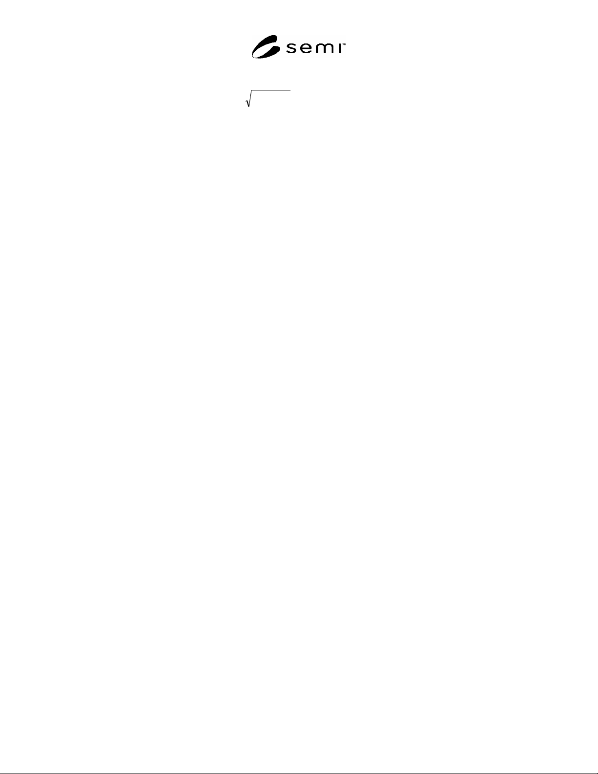
A1-10.5 Calculate and record the scanner XY uncertainty as follows:
)(
22
yx
SSS (A4)
NOTICE: SEMI makes no warranties or representations as to the suitability of the standards set forth herein for any
particular application. The determination of the suitability of the standard is solely the responsibility of the user.
Users are cautioned to refer to manufacturer's instructions, product labels, product data sheets, and other relevant
literature, respecting any materials or equipment mentioned herein. These standards are subject to change without
notice.
By publication of this standard, Semiconductor Equipment and Materials International (SEMI) takes no position
respecting the validity of any patent rights or copyrights asserted in connection with any items mentioned in this
standard. Users of this standard are expressly advised that determination of any such patent rights or copyrights, and
the risk of infringement of such rights are entirely their own responsibility.
Copyright by SEMI® (Semiconductor Equipment and Materials
International), 3081 Zanker Road, San Jose, CA 95134. Reproduction of
the contents in whole or in part is forbidden without express written
consent of SEMI.
SEMI M51-0303 © SEMI 2002, 2003 1
SEMI M51-0303
TEST METHOD FOR CHARACTERIZING SILICON WAFERS BY GATE
OXIDE INTEGRITY
This test method was technically approved by the Global Silicon Wafer Committee and is the direct
responsibility of the Japanese Silicon Wafer Committee. Current edition approved by the Japanese Regional
Standards Committee on January 10, 2003. Initially available at www.semi.org January 2003; to be
published March 2003. Originally published July 2002.
NOTICE: This document was rewritten in its entirety
in 2002.
1 Purpose
1.1 This test method describes procedures for
characterizing silicon wafers to determine Gate Oxide
Integrity (GOI). This test method is effective in
evaluating the density of Crystal Originated Particles
(COP) in polished Czochralski (CZ) silicon wafers that
influence GOI.
2 Scope
2.1 This test method provides detailed procedures for
characterizing silicon wafers using GOI. This test
method describes standard procedures for Metal Oxide
Semiconductor (MOS) fabrication, electrical
measurement, analysis, and reporting.
2.2 Thermally grown gate oxide films with gate oxide
thicknesses ranging from 20–25 nm and polysilicon
electrodes are used as MOS capacitors. Discussion of
the gate oxide thickness is given in a later section.
2.3 Time Zero Dielectric Breakdown (TZDB) is used
as the electrical characterization method of MOS
capacitors.
2.4 It is well known that oxygen precipitates are also a
source of gate oxide defects.
1
However, this is beyond
the scope of this standard because the as-received
wafers contain only a small amount of oxygen
precipitate.
NOTE 1: The polysilicon film can make standard test results
applicable to the testing of wafers used to fabricate integrated
circuits rather than other metal electrodes because polysilicon
electrodes are commonly used in actual devices.
NOTE 2: The TZDB method measures oxide breakdown
electric fields using MOS capacitors. The density of COPs
can be estimated from a histogram of the breakdown electric
field.
NOTE 3: For a detailed discussion of sample structures for
this test method, the reader is referred to EIA/JEDEC
Standard 35-1. In general, the three most likely sample
1 K.Yamabe and K.Taniguchi, “Time-Dependent Dielectric
Breakdown of Thin Thermally Grown SiO2 Films”, J. Solid St.
Circuits, SC-20, 343 (1983).
structures are simple planar MOS capacitors, MOS capacitors
with various isolation structures (for example, local oxidation
of silicon (LOCOS), shallow trench isolation (STI)), and field
effect transistors (FET). For the purpose of silicon wafer
characterization, the simple planar MOS capacitor structure is
preferable. This is because with the various isolation
structures and FET, silicon wafers sometimes receive thermal
treatments during the complicated sample fabrication process.
Therefore, it is questionable to look upon a measurement of
one of the latter two wafers as the starting silicon wafer
characterization.
NOTE 4: This standard is based on round robin results
among silicon wafer manufacturers. In general, the COPs in
the polished CZ silicon substrates strongly influence the
TZDB histogram of the gate oxide. This GOI test method
strongly depends on wafer-surface/near-surface crystal
defects, contaminations, particles and cleanliness of the MOS
fabrication processes environment. Cleanliness of the
processes environment should be evaluated because it
strongly affects the MOS characteristics. (See Section 5.2.1
and Related Information 1).
NOTICE: This standard does not purport to address
safety issues, if any, associated with its use. It is the
responsibility of the users of this standard to establish
appropriate safety and health practices and determine
the applicability of regulatory or other limitations prior
to use.
3 Referenced Standards
3.1 SEMI Standards
SEMI C3.6 ― Standard for Phosphine in Cylinders
99.98% Quality (Provisional)
SEMI C3.21 ― Standard for Carbon Tetrafluoride in
Cylinders (Provisional)
SEMI C3.22 ― Standard for Oxygen, 99.5% Quality
SEMI C3.23 ― Standard for Oxygen, 99.98% Quality
SEMI C3.28 ― Standard for Nitrogen, VLSI Grade in
Cylinders, 99.9996% Quality
SEMI C3.41 ― Standard for Oxygen, Bulk, 99.9998%
Quality (Provisional)
SEMI C3.49 ― Standard for Bulk Nitrogen,
99.99999% Quality (Provisional)
SEMI C3.54 ― Gas Purity Guideline for Silane

SEMI M51-0303 © SEMI 2002, 2003 2
SEMI C21 ― Specifications and Guidelines for
Ammonium Hydroxide
SEMI C27 ― Specifications and Guidelines for
Hydrochloric Acid
SEMI C28 ― Specifications and Guidelines for
Hydrochloric Acid
SEMI C30 ― Specifications and Guidelines for
Hydrogen Peroxide
SEMI C35 ― Specifications and Guidelines for Nitric
Acid
SEMI C38 ― Guideline for Phosphorus Oxychloride
SEMI C41 ― Specifications and Guidelines for 2-
Propanol
SEMI C44 ― Specifications and Guidelines for
Sulphuric Acid
SEMI M1 — Specifications for Polished Monocrys-
talline Silicon Wafers
3.2 ASTM Standards
2
ASTM D5127 ― Standard Guide for Ultra Pure Water
Used in the Electronics and Semiconductor Industry
ASTM F1241 ― Terminology of Silicon Technology
ASTM F1771 ― Standard Test Method for Evaluating
Gate Oxide Integrity by Voltage Ramp Technique
3.3 EIA/JEDEC Standards
3,
4
EIA/JEDEC 35 ― Procedure for the Wafer-Level
Testing of Thin Dielectrics
EIA/JEDEC 35-1 ― General Guidelines for Designing
Test Structures for the Wafer-Level Testing of Thin
Dielectrics
EIA/JEDEC 35-2 ― Test Criteria for the Wafer-Level
Testing of Thin Dielectrics
NOTICE: Unless otherwise indicated, all documents
cited shall be the latest published versions.
4 Terminology
4.1 Abbreviations & Acronyms
4.1.1 COPs — Crystal Originated Particles
2 American Society for Testing and Materials, 100 Barr Harbor
Drive, West Conshohocken, Pennsylvania 19428-2959, USA.
Telephone: 610.832.9585, Fax: 610.832.9555 Website:
www.astm.org
3 Electronic Industries Alliance, EIA Engineering Department,
Standards Sales Office, 2001 Eye Street, NW, Washington, D.C.
20006, USA. Website: www.eia.org
4 Joint Electron Device Engineering Council, 2500 Wilson Blvd.,
Arlington, VA 22201, website: www.jedec.org
4.1.2 GOI — Gate Oxide Integrity
4.1.3 LOCOS — LOCal Oxidation of Silicon
4.1.4 MOS — Metal Oxide Semiconductor
4.1.5 STI — Shallow Trench Isolation
4.1.6 TZDB — Time Zero Dielectric Breakdown
4.2 Definitions
4.2.1 Many terms relating to silicon technology are
defined in ASTM Terminology F1241.
4.2.2 Definitions for some additional terms are given in
SEMI M1 and ASTM F1771.
4.2.3 Other terms are defined as follows:
4.2.3.1 crystal originated particles
5
(COPs) — this is
one of the grown-in defects of CZ silicon wafers with
an octahedral structure. It was discovered as particles
appeared on the silicon surface during repetitive RCA
SC-1
6
cleaning.
NOTE 5: It has been thought that COPs are one of the main
origins of GOI degradation. The gate oxide formed on the
silicon surface at which the COPs appear breaks down easily
at the corner of an octahedral shape like a silicon trench.
7, 8
The oxide electric field is enhanced at that place. The
breakdown electric field is weakened.
4.2.3.2 failure modes ― The breakdown failure results
are summarized in terms of the range of the oxide
electric field in which the breakdown occurred. One set
of categories (A, B and C for TZDB) widely used
9, 10
is
as follows:
• A mode failure: 0 MV/cm ≤ E
bd
< 3 MV/cm
• B mode failure: 3 MV/cm ≤ E
bd
< 8MV/cm
• C mode failure: 8 MV/cm ≤ E
bd
NOTE 6: Discussion on failure modes:
• A mode failure: Initial short
5 J. Ryuta, E. Morita, T. Tanaka and Y. Shimanuki, “Crystal –
Originated Singularities on Si Wafer Surface after SC1 Cleaning”,
Jpn. J. Appl. Phys. 29(1990) L1947.
6 W. Kern and D. Puotinen, “Clean Solution Based on Hydrogen
Peroxide for Use in Silicon Semiconductor Technology”, RCA Rev.,
31, 187(1970).
7 T. Mera, J. Jablonski, K. Nagai, and M. Watanabe, “Grown-in
defects in silicon crystals responsible for gate oxide integrity
deterioration”, Ohyo-Buturi, 66(7), 728 (1997).
8 K.Yamabe and K.Imai, “Nonplanar Oxidation and Reduction of
Oxide Leakage Currents at Silicon Corners by Rounding-off
Oxidation”, IEEE Trans. Electron Devices, ED-34,1681 (1987) .
9 K. Yamabe, K. Taniguchi, and Y. Matsushita, “Thickness
Dependence of Dielectric Breakdown Failure of Thermal SiO2
Films”, Reliability Physics – 21st Annual Proceedings, 1983, p.184.
10 K. Yamabe, Y. Ozawa, S. Nadahara, and K. Imai, “Thermally
Grown Silicon Dioxide with High Reliability”, in “Semiconductor
Silicon 1990”, ECS Proceedings Volume 90-1, pp. 349-363.