semi合集-English.pdf - 第5012页
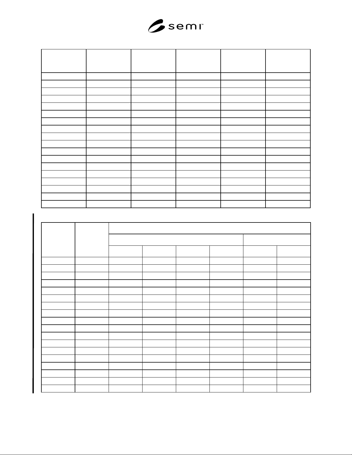
SEMI M17-0704 © SEMI 1990, 2004 3 Table 1 Grid Element Scheme Circle Number Number of Divisions Included Angle Total Number of Divisions Included Area Ratio Relative Diameter 01 4 90.0° 4 0.004 0.0632 02 8 45.0° 12 0.012…

SEMI M17-0704 © SEMI 1990, 2004 2
actual diameter of any circle, multiply the relative
diameter by the outer diameter of the grid.
5.1.2 The outer diameter of the grid is chosen to be the
size appropriate for a particular application. This
diameter would normally be chosen to be the nominal
diameter of the fixed quality area to allow for such
things as an edge exclusion, tolerance variations in the
wafer diameter, and edge rounding. Table 2 shows the
circle diameters for a series of grids which have a fixed
quality area radius 3 or 4 mm smaller than the nominal
radius of selected wafers specified in SEMI M1.
5.1.3 Identification of each grid element is done by
referring to a circle number and a division number on
that circle. Circles are numbered from the center out,
with the center circle being number 01 and the
outermost circle being number 18. The divisions are
numbered starting with the first division
counterclockwise from the horizontal line which starts
at the center of the grid and extends to the right, when
the primary fiducial (flat or notch) is placed at the
bottom of the grid. Divisions are progressively
numbered counterclockwise from 01 to n, where n
equals the total number of divisions on the circle. An
element’s address is given by two sets of numbers
separated by a comma: circle (0–18), division (01–n).
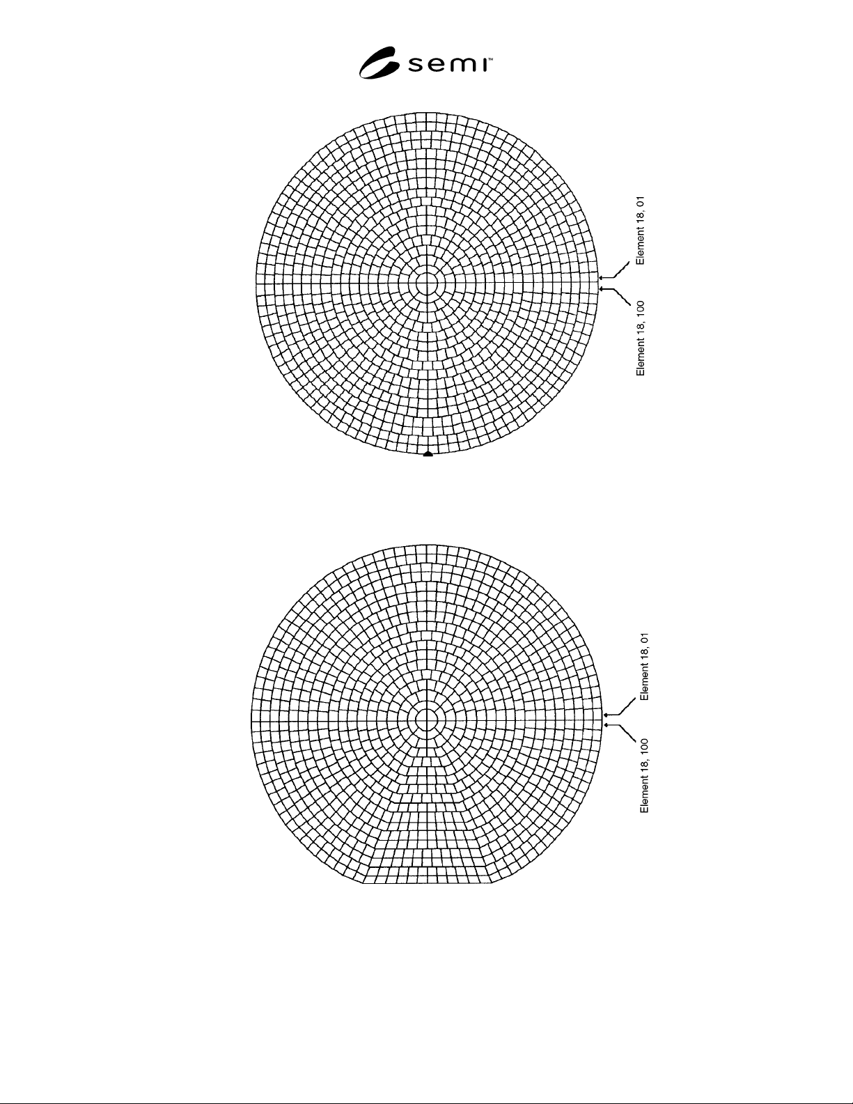
Elements 18, 01 and 18, 100 are identified in Figure 1.
5.2 Wafers without a Primary Flat
5.2.1 The grid elements for wafers without a primary
flat are illustrated in Figure 1. This pattern is generated
by making concentric circles with relative diameters
and radial divisions as specified in Table 1. In this table
the circle number is given in the leftmost column. The
number of divisions and the included angle of each
division in the circle are given in the second and third
columns. The total number of divisions (from the center
outward) is given in the fourth column. The included
area ratio, given in the fifth column, is the total number
of divisions included within a circle divided by 1000,
the total number of divisions in the grid. The relative
diameter, given in the rightmost column, is the square
root of the included area ratio.
5.3 Wafers with a Primary Flat
5.3.1 For wafers with a primary flat, a standard
included angle of 43.2° is used for all wafer sizes. This
angle was chosen because it lies between the maximum
and minimum included angles of the primary flats
specified in SEMI M1 for 100 mm, 125 mm, 150 mm,
and 200 mm diameter wafers. In addition, if a fixed
quality area of radius 3 mm less than the nominal wafer
radius (or smaller) is used, the grid will not in any case
extend beyond the edge of the wafer in the region of the
primary flat.
5.3.2 This flat is propagated into the wafer as
illustrated in Figure 2. The diameter of each circle is the
same as for wafers without a primary flat. The flat is
propagated vertically downward (starting with circle
number 3) by the intersection of the circle with a
horizontal chord which subtends 43.2° .
5.3.3 The areas of the grid elements within the
propagated flat region are slightly smaller than the areas
of the regular grid elements. This difference is ignored
when counting grid elements for wafers with a primary
flat. All grid elements are assumed to be 0.001 of the
total fixed quality area.
5.4 Secondary Flats
5.4.1 The grid ignores secondary flats. These are
shallow enough that the outer circle does not extend
beyond the wafer edge if a fixed quality area of radius 3
mm less than the nominal wafer radius is used.
NOTE 1: In this sense, the fixed quality area used by the
Universal Wafer Grid deviates somewhat from the formal
definition in SEMI M1 which embodies an edge exclusion of
constant width around the entire periphery of the wafer
including the region of the secondary flat.
6 Use of the Grid
6.1 The quantification of defective area is done by
overlaying a transparency of the grid onto a map of
wafer defects or by mapping observed defects onto the
grid. The number of grid elements which contain
defects is counted. The element count divided by 10
corresponds to the percent of defective area. This grid
could also be superimposed onto a CRT display,
photograph, or computer generated map, where
applicable. In use, grid pattern diameters must be
scaled to the size of the map or image of the wafer to be
overlaid.
SEMI M17-0704 © SEMI 1990, 2004 3
Table 1 Grid Element Scheme
Circle
Number
Number
of Divisions
Included
Angle
Total
Number
of Divisions
Included
Area Ratio
Relative
Diameter
01 4 90.0° 4 0.004 0.0632
02 8 45.0° 12 0.012 0.1095
03 16 22.5° 28 0.028 0.1673
04 24 15.0° 52 0.052 0.2280
05 30 12.0° 82 0.082 0.2864
06 36 10.0° 118 0.118 0.3435
07 40 9.0° 158 0.158 0.3975
08 48 7.5° 206 0.206 0.4539
09 50 7.2° 256 0.256 0.5060
10 60 6.0° 316 0.316 0.5621
11 72 5.0° 388 0.388 0.6229
12 72 5.0° 460 0.460 0.6782
13 80 4.5° 540 0.540 0.7348
14 80 4.5° 620 0.620 0.7874
15 90 4.0° 710 0.710 0.8426
16 90 4.0° 800 0.800 0.8944
17 100 3.6° 900 0.900 0.9487
18 100 3.6° 1000 1.000 1.0000
Table 2 Grid Circle Diameters (in mm) for Various Standard Wafer Sizes with Nominal Edge Exclusion, E.
Nominal Wafer Diameter
E = 3 mm E = 4 mm
Circle Number
Relative
Diameter
100 mm 125 mm 150 mm 200 mm 150 mm 200 mm
01 0.0632 5.94 7.52 9.10 12.26 8.97 12.13
02 0.1095 10.29 13.03 15.77 21.24 15.55 21.02
03 0.1673 15.73 19.91 24.09 32.46 23.76 32.12
04 0.2280 21.43 27.13 32.83 44.23 32.38 43.78
05 0.2864 26.92 34.08 41.24 55.56 40.67 54.99
06 0.3435 32.29 40.88 49.46 66.64 48.78 65.95
07 0.3975 37.37 47.30 57.24 77.12 56.45 76.32
08 0.4539 42.67 54.01 65.36 88.06 64.45 87.15
09 0.5060 47.56 60.21 72.86 98.16 71.85 97.15
10 0.5621 52.84 66.89 80.94 109.05 79.82 107.92
11 0.6229 58.55 74.13 89.70 120.84 88.45 119.60
12 0.6782 63.75 80.71 97.66 131.57 96.30 130.21
13 0.7348 69.07 87.44 105.81 142.55 104.34 141.08
14 0.7874 74.02 93.70 113.39 152.76 111.81 151.18
15 0.8426 79.20 100.27 121.33 163.46 119.65 161.78
16 0.8944 84.07 106.43 128.79 173.51 127.00 171.72
17 0.9487 89.18 112.90 136.61 184.05 134.72 182.15
18 1.0000 94.00 119.00 144.00 194.00 142.00 192.00
SEMI M17-0704 © SEMI 1990, 2004 4
Figure 1
Grid Layout for Wafers Without a Primary Flat
Figure 2
Grid Layout for Wafers With a Primary Flat