semi合集-English.pdf - 第7615页
6.4.5 The distance from the edge of the data matrix code sym bol to the diameter perpendicul ar to the prim ar y fiducial bisector varies accor ding to the act ual size of the wafer and the placement of the symbol within…
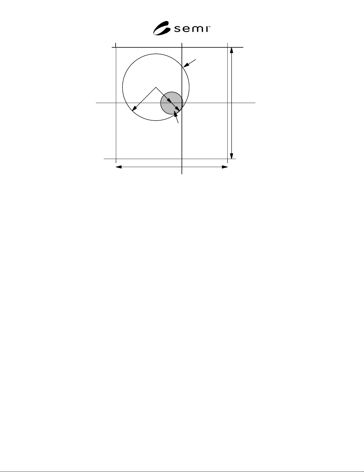
Dot
Central Area of Cell
45
20
25
Rdot (min) = 45
Rcentral area (min) = 25
Rdot misalign (max) = 20
100
100
Figure 4
Minimum Size Dot with Maximum Dot Misalignments (all Dimensions in µm)
6.3 Content of the Matrix Code Symbol
6.3.1 Each square matrix code symbol shall contain between 10 and 23 message characters encoded in accordance
with AIM ISS Data Matrix, including the characters associated with error checking and correcting (ECC200), as
also defined in AIM ISS Data Matrix.
6.3.2 The message characters may include any of those designated as “mostly uppercase” in Table 5 and Annex J of
AIM ISS - Data Matrix. The first 10 message characters shall contain two elements:
a vendor-assigned 8-character wafer identification code, followed by
a 2-character vendor identification code as defined in SEMI AUX001.
6.3.2.1 The remaining message characters, if any, shall contain information as agreed between the vendor and user.
6.3.3 The total number of message characters available depends on the row/column count and on the encoded
character set (see Table 2).
6.4 Location of the Matrix Code Symbol
6.4.1 With the wafer positioned front surface up and with the primary fiducial toward the operator, the reference
point of the matrix code symbol shall be located as specified in Table 3.
6.4.2 The square matrix code symbol used on 125 to 200 mm diameter wafers shall be oriented with the border
columns parallel with the primary fiducial bisector and the border rows perpendicular to the primary fiducial
bisector. The secondary border column shall be toward the primary fiducial bisector, and the primary border row
shall be toward the edge of the wafer.
6.4.3 The nominal position of the reference point of the matrix code symbol is 1 mm to the right of the closest
alphanumeric code field. A 3º skew toward the alphanumeric field, which is the maximum skew allowed by SEMI
M12 and SEMI M13, does not cause the matrix code symbol to impinge on the alphanumeric code fields, even if the
symbol is placed only 15.5 mm from the primary fiducial bi-sector. Consequently, this matrix code symbol position
permits the simultaneous use of front surface alphanumeric marking as specified in SEMI M12 or M13, on 125 to
200 mm wafers with either flatted or notched primary fiducials.
6.4.4 Because the matrix code symbol is located in the same place with respect to the primary fiducial bisector on
all wafer diameters from 125 to 200 mm, the use of both marking and reading equipment is simplified.
SEMI T2-0298 © SEMI 1993, 2004 5
6.4.5 The distance from the edge of the data matrix code symbol to the diameter perpendicular to the primary
fiducial bisector varies according to the actual size of the wafer and the placement of the symbol within its tolerance
range. Minimum distances from the edge of the code symbol to the wafer center-line are given in Table 4 for both
16 × 16, 125 µm and 20 × 20, 150 µm matrix code symbols.
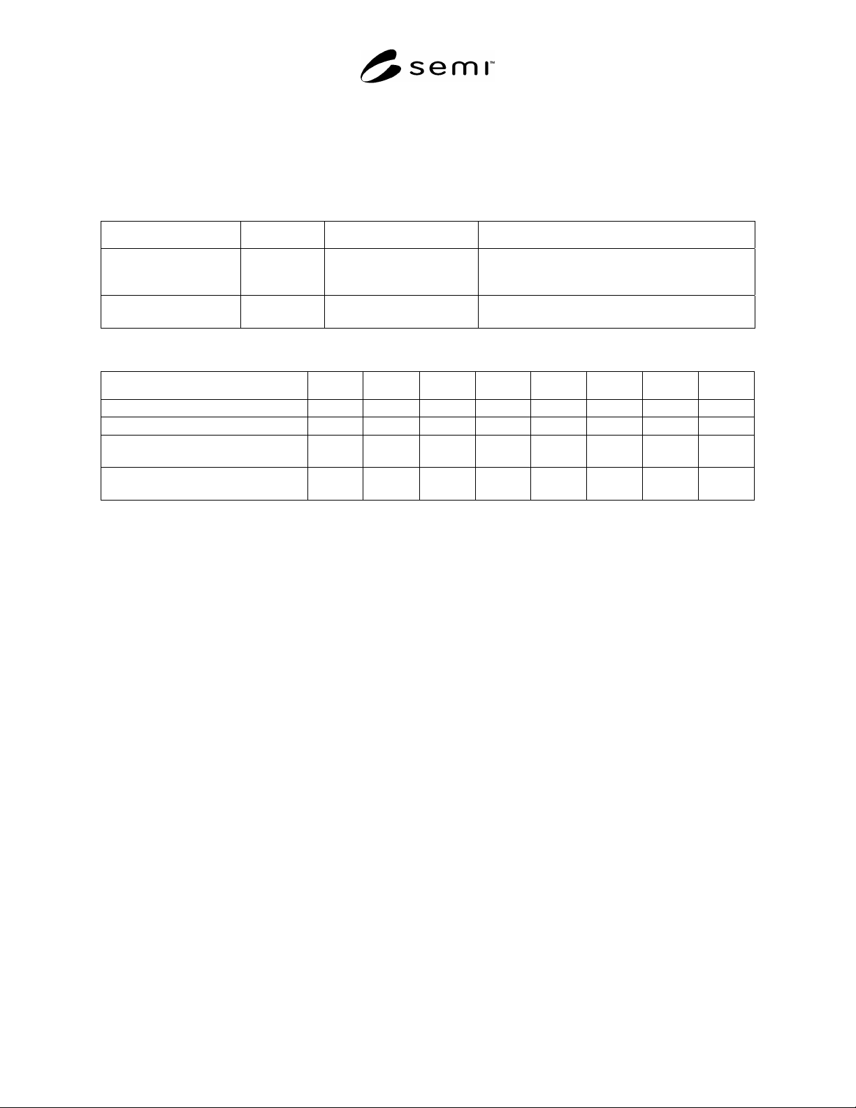
Table 3 Location of Matrix Code Symbol — Wafer Polished Side Up, Primary Fiducial toward the Operator
Type of Array Wafer Fiducial Reference Point Cell Location of Symbol Reference Point
Square (used on 125, 150,
and 200 mm wafers)
Flat Common cell of primary
border row and secondary
border column
16.0 ± 0.5 mm to the right of the fiducial bisection,
and 2.5 ± 0.5 mm above the edge of the flat
Notch 160 ± 0.5 mm to the right of the fiducial bisector, and
5.3 ± 0.5 mm above the notch pin center
Table 4 Minimum Distances from Edge of Matrix Code Symbol to the Wafer Centerline
SEMI Standard M1.7 M1.8 M1.12 M1.13 M1.10 M1.9
Nominal Wafer Diameter, mm 125 150 125 150 200 125 150 200
Flat or Notch Flat Flat Flat Flat Flat Notch Notch Notch
Distance from 20 × 20 Matrix with 150
µm Cell Spacing, mm
52.17 62.76 52.33 64.73 89.28 53.98 66.48 91.48
Distance from 16 × 16 Matrix with 125
µm Cell Spacing, mm
53.14 63.73 53.30 65.74 90.25 54.95 67.45 92.45
SEMI T2-0298 © SEMI 1993, 2004 6

APPENDIX 1
SIMULTANEOUS MARKING WITH SQUARE DATA MATRIX AND
ALPHANUMERIC CODES
NOTICE: The material in this appendix is an official part of SEMI T2 and was approved by full letter ballot
procedures.
A1-1 The relative positions of alphanumeric and data matrix markings are shown in Figure A1-1. This figure also
shows the relationship between the data matrix code symbol and the edge of the polished area of the front surface of
the wafer. Wafer peripheries in the figure are the edges of the polished area of wafers with maximum intrusion of
the edge contour, minimum diameter, and maximum flat diameter (minimum flat length), or distance between the
notch pin centerline and the wafer edge, as specified in SEMI M1. For all wafer diameters, SEMI M1 allows the
edge contour to extend inward from the edge up to 508 µm (Dimension B in Figure 4 of SEMI M1). The distance
between the notch pin centerline and the wafer periphery may vary from 0.30 to 0.80 mm as indicated in Figure 6 of
SEMI M1. Other dimensions and tolerances are specified in the appropriate polished wafer specification in SEMI
M1.
A1-2 Alphanumeric code field locations are shown for all cases except the SEMI M13 code field for flatted wafers,
which lies entirely to the left of the primary fiducial bisector. Note that alphanumeric code field locations are not
specified for 125 mm diameter notched wafers in either SEMI M12 or SEMI M13.
A1-3 The nominal position of the reference point of the data matrix code symbol is marked by a +; this position is 1
mm to the right of the closest alphanumeric code field. Because of the tolerances on the position of the reference
point, the largest data matrix code symbol (20 × 20, 150 µm cell spacing) may lie anywhere within the dotted
square. The effect of a 3º skew toward the alphanumeric field is also shown. Although the skew does not affect
readability of the data matrix code symbol, too great a skew may cause the data matrix symbol code to impinge on
occupied areas of the wafer surface. The 3º skew, which is the maximum allowed by SEMI M12 and SEMI M13,
does not cause the data matrix code symbol to impinge on the alphanumeric code fields.
SEMI T2-0298 © SEMI 1993, 2004 7