semi合集-English.pdf - 第5378页
SEMI M55.1-0304 © SEMI 2004 1 SEMI M55.1-0304 SPECIFICATION FOR 50. 8 mm ROUND POLISHED MONOCRYSTALLINE 4H AND 6H SILICON CARBIDE WAFERS This specification was technically approved b y th e Global Compound Sem iconductor…
SEMI M55-0705 © SEMI 2003, 2004 11
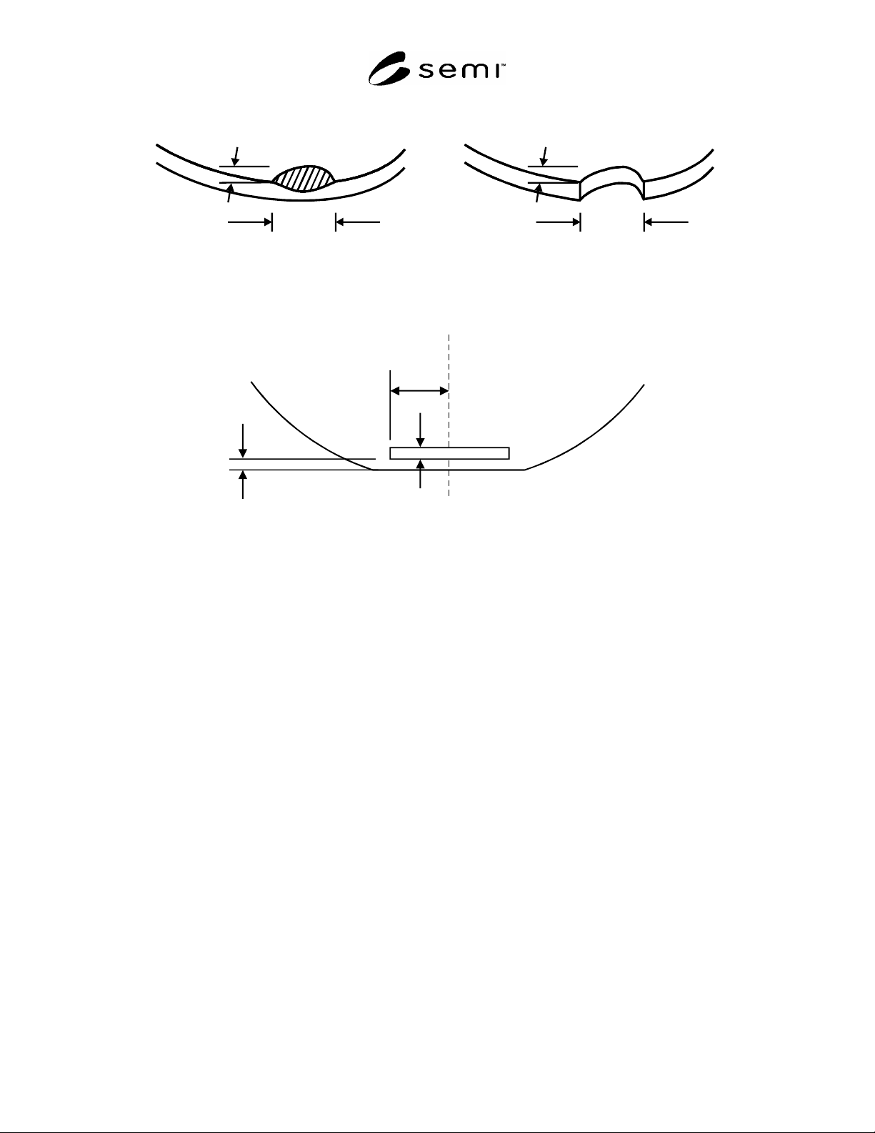
length
depth
indent
length
edge chip
depth
Figure 7
Depth and length of edge chip and indent
Backside
Primary Flat
A
C
C
L
B
characters
Figure 8
Definition of Window for Laser Marking
The width of the permitted window is twice dimension C.
NOTE 15: For the exact dimensions of A, B, and C, see the appropriate wafer standard.
NOTICE: SEMI makes no warranties or representations as to the suitability of the standards set forth herein for any
particular application. The determination of the suitability of the standard is solely the responsibility of the user.
Users are cautioned to refer to manufacturer's instructions, product labels, product data sheets, and other relevant
literature, respecting any materials or equipment mentioned herein. These standards are subject to change without
notice.
By publication of this standard, Semiconductor Equipment and Materials International (SEMI) takes no position
respecting the validity of any patent rights or copyrights asserted in connection with any items mentioned in this
standard. Users of this standard are expressly advised that determination of any such patent rights or copyrights, and
the risk of infringement of such rights are entirely their own responsibility.
Copyright by SEMI® (Semiconductor Equipment and Materials
International), 3081 Zanker Road, San Jose, CA 95134. Reproduction of
the contents in whole or in part is forbidden without express written
consent of SEMI.
SEMI M55.1-0304 © SEMI 2004 1
SEMI M55.1-0304
SPECIFICATION FOR 50.8 mm ROUND POLISHED
MONOCRYSTALLINE 4H AND 6H SILICON CARBIDE WAFERS
This specification was technically approved by the Global Compound Semiconductor Committee and is the
direct responsibility of the European Compound Semiconductor Materials Committee. Current edition
approved by the European Regional Standards Committee on October 29, 2003. Initially available at
www.semi.org January 2004; to be published March 2004.
NOTE 1: This specification is intended to be a sub-document to SEMI M55, Specification For Polished Monocrystalline Silicon
Carbide Wafers.
1 Purpose
1.1 This subordinate standard details the dimensional values and other information required for 50.8 mm polished
monocrystalline silicon carbide wafers.
2 Scope
2.1 The complete specification for this product includes all general requirements of SEMI M55, Specification For
Polished Monocrystalline Silicon Carbide Wafers.
NOTICE: This standard does not purport to address safety issues, if any, associated with its use. It is the
responsibility of the users of this standard to establish appropriate safety and health practices and determine the
applicability of regulatory or other limitations prior to use.
3 Limitations
3.1 The backside finish properties, dopant, and resistivity are not addressed, as currently these properties depend
strongly on the quick evolving technology and suitable limits for a standard do not exist.
4 Requirements
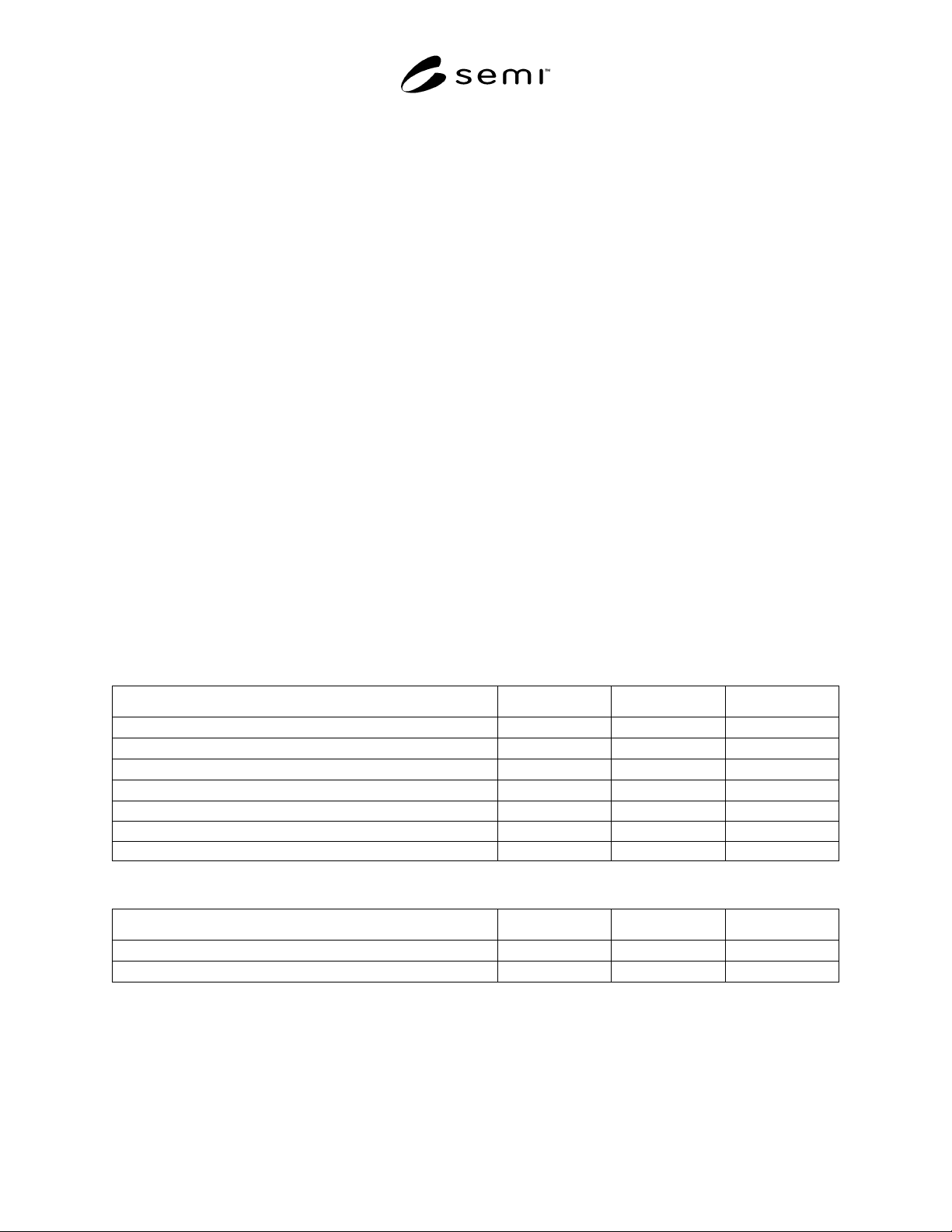
Table 1 Dimension and Tolerance Requirements
Property Dimension Tolerance Units
DIAMETER 50.8
± 0.25
mm
PRIMARY FLAT LENGTH 15.8
± 1.6
mm
SECONDARY FLAT LENGTH 8.0
± 1.6
mm
BOW 0
± 25
µ m
WARP 0 < 25 µ m
TOTAL THICKNESS VARIATION 0 < 25 µ m
TOTAL INDICATOR READING 0 < 25 µ m
Table 2 Thickness Requirements (Center Point)
Dimension Tolerance Units
Option 1: 250
± 25
µ m
Option 2: 330
± 25
µ m
NOTE 1: As the industrial requirements for a unique thickness specification are not established at the time of creation of this standard, two
values are defined. This is to be regarded as a preliminary in that way, that in a future revision of this standard these options can be expected to
be replaced by a unique definition.
SEMI M55.1-0304 © SEMI 2004 2
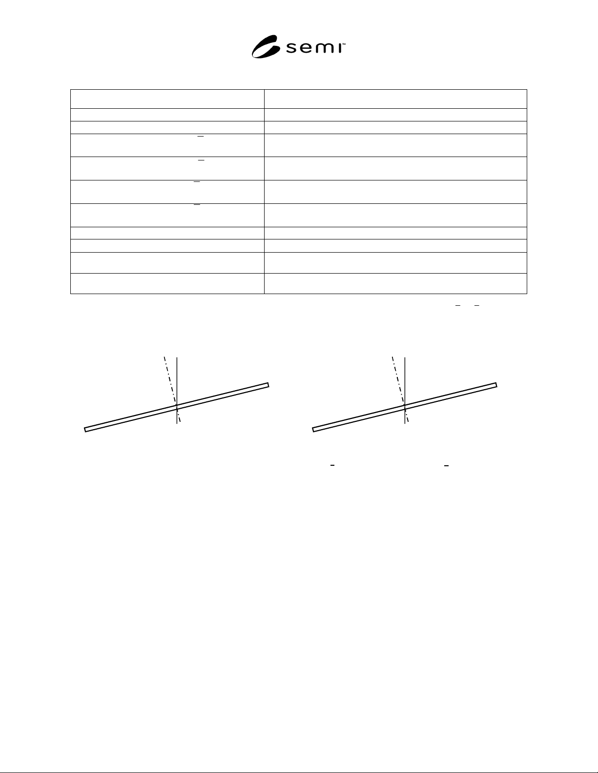
Table 3 Orientation and Flat Location Requirements
Property Dimension
SURFACE ORIENTATION
(see Note 1)
Tilt angle (see Figure 2 in SEMI M55)
Option 1: “on axis”
0 + 0.25°
Option 2: “off axis (1120)”
3.5° ± 0.5° parallel to edge of primary flat away from secondary flat
(see Note 1)
Option 3: “off axis (1120)”
8.0° ± 0.5° parallel to edge of primary flat away from secondary flat
(see Note 1)
Option 4: “off axis (1100)”
3.5° ± 0.5° parallel to edge of secondary flat away from primary flat
(see Note 1)
Option 5: “off axis (1100)”
8.0° ± 0.5° parallel to edge of secondary flat away from primary flat
(see Note 1)
ORTHOGONAL MISORIENTATION
± 5° (See Figure 2 in SEMI M55)
TOLERANCE OF PRIMARY FLAT
ORIENTATION
± 1°
TOLERANCE OF SECONDARY FLAT
ORIENTATION (see Note 4)
± 5° relative to primary flat
NOTE 1: The frame of reference is the (0001)-plane of the crystal. It is the wafer normal on the silicon-face that is tilted towards the given
crystallographic direction. That means that the crystallographic c-axis lies between the secondary/primary flat (for the (1120)/(1100) option) and
the silicon-face surface normal vector (See Figure 1 and 2).
NOTE 2: The angle between primary and secondary flat is defined in Figure 5 in SEMI M55.
Secondary flat
Si-face
Normal vector to
wafer surface
Crystallographic
c-axis
C-face
Primary flat
Si-face
Normal vector to
wafer surface
Crystallographic
c-axis
C-face
Figure 1
Definition of the Sign of the Tilt Angle (left: off axis (1120) -option, right off axis (1100) Option)