semi合集-English.pdf - 第6163页
SEMI G34-89 © SEMI 198 6, 1996 3 9.5 Solderability — Per MIL- ST D - 8 83 , Method 2003. 9.6 Seque nce of Events and Incom i n g Testing — During incoming ins p ection, the sequ e nce of testing shall be: 1. Fram e A tta…
SEMI G34-89 © SEMI 1986, 1996 2
6.1.2 Color — Black, dark brown, o r dark violet.
6.2 Sealing Material — Solder glass designed to form
a hermetic seal. Glass type and temperature/time profile
shall be specified.
6.3 Die Attach Pad — Gold (or ot her suitable
material).
6.4 Leadframe — Fully annealed Alloy 42.
6.5 Lead Finish — Unless otherw ise specified, hot tin-
lead solder dip, Type A, per MIL-M-38510, to within
0.030" of lead seal on plated leads, and 100% coverage
if applied directly over base metal.
7 Defect Limits
7.1 Ceramic
7.1.1 Cracks — Cracks are not allowed.
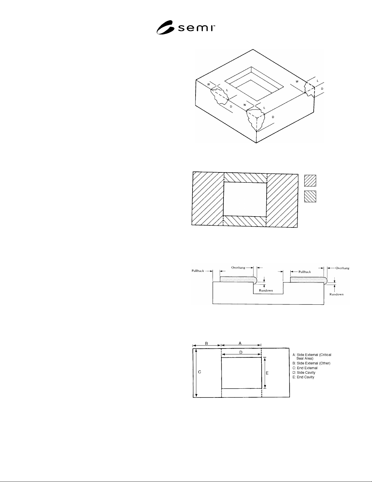
7.1.2 Chips — See Figures 1 and 2.
7.1.2.1 Corner Chips — 0.762 mm (0.030") × 0.762
mm (0.030") × 25% of package element thickness.
7.1.2.2 Edge Chips — 2.54 mm (0.060") × 0.762 mm
(0.030") × 25% of package element thickness.
7.1.2.3 Critical Seal Area — Chips ca nnot reduce the
critical seal path to less than half the nominal design
dimension at any point. No more than four chips are
allowed in the critical seal area.
7.1.3 Burrs, Projections, and Fins
7.1.3.1 Cap — 0.127 mm (0.005") maximum.
7.1.3.2 Base — 0.076 mm (0.003") ma ximum.
7.1.3.3 Die Attach Surface — 0.025 mm (0.001")
maximum above metallization excluding a 0.254 mm
(0.010") perimeter.
7.1.4 Camber — 0.050 mm (0.002") camber permitted
up to maximum of 0.004 inch/inch (mm/mm).
7.2 Glass
7.2.1 Chips or Voids — Chips in the glass or missing
glass is allowed, provided the region of the chipped or
missing glass meets the minimum specified glass
thickness after melting the glass as specified.
7.2.2 Glass Misalignment — (after glass flow) (see
Figure 3.)
7.2.2.1 External Overhang — 0.127 m m (0.005")
maximum.
7.2.2.2 External Rundown — 30% of ceramic
thickness maximum.
7.2.2.3 Pullback — See Table 1 and Figures 2, 3, and
4.
Table 1 Maximum Allowable Pullback
Side external (critical seal) 0.010" (2.54 mm)
Side external (other) 0.015" (0.381 mm)
End external 0.020" (0.508 mm)
Side cavity 0.010" (0.254 mm)
End cavity 0.010" (0.254 mm)
NOTE: Maximum allowable critical seal area reduction on
any one side between side cavity and side external shall not
reduce critical seal path to less than 0.635 mm (0.025").
8 Sampling
Sampling will be determined between supplier and
purchaser.
9 Functional Test Methods
9.1 Die Attach Quality
9.1.1 Visually inspect preform weto ut after die attach.
Minimum fillet shall be 75% of the die perimeter.
9.1.2 Perform destructive die shear t est post
environmental testing per MIL-STD-883, Method 2019.
9.1.3 Inspect to reveal voids in the d ie attach eutectic
alloy or approved silver-filled glass per MIL-STD-883,
Method 2012.
9.2 Lead Bond Quality — Perform minimum pre-seal
and post-seal bond strength test per MIL-STD-883,
Method 2011, Test Condition D. Reject for bonds
causing the metallization to lift from the leadframe
post.
9.3 Hermetic Environmental Testi ng
9.3.1 The hermetic integrity of the p ackage must be
maintained after all environmental testing. Hermetic
check shall comply with MIL-STD-883, Method 1014,
Test Condition A, or B and C.
9.3.2 Environmental testing shall inc lude, but not be
limited to, the following:
9.3.2.1 Temperature Cycle per MIL-STD-883, Method
1010, Condition C.
9.3.2.2 Thermal Shock per MIL-STD-883, Method
1011, Condition B.
9.3.2.3 Centrifuge per MIL-STD-883, Method 2001,
Condition D, Y axis only.
9.3.2.4 Moisture Resistance per MIL-S TD-883,
Method 1004.
9.4 Die Attach Material Thickness — Die attach
material thickness shall be measured by standard cross-
sectioning without smearing.
SEMI G34-89 © SEMI 1986, 19963
9.5 Solderability — Per MIL-STD-883, Method 2003.
9.6 Sequence of Events and Incoming Testing —
During incoming inspection, the sequence of testing
shall be:
1. Frame Attach
2. Die Attach
3. Bond (if applicable)
4. Seal
5. Lead Finish (Type A per MIL-M-38510)
6. Environmental Testing
7. Lead Trim
8. Fine Leak
9. Gross Leak
10. Torque Test (test method pending)
11. Bond Pull
12. Die Shear (optional)
9.6.1 Solderability — A separate sample with lead
finish Type A shall be subjected to preconditioning of
Class B time/temperature exposure per burn-in Test
Method 1015, MIL-STD-883, then tested to Method
2003.
NOTE: An initial qualification on the thermal and electrical
characteristics of the package may be performed. The
characteristics tested will be:
Insulation Resistance — Per MIL-STD-883, Method
1003, Test Condition B.
Thermal Dissipation — Per MIL-STD-883, Method
1012.
10 Packaging and Marking
10.1 Packaging — Containers selec ted shall be strong
enough and suitably designed to provide maximum
protection against crushing, spillage, and other forms of
damage to the container or its contents. Containers shall
afford protection of the contents from contamination
and exposure to excessive moisture or oxidation by
gases. Packaging materials shall be so selected to
prevent any contamination of the ceramic component
parts with paper fibers or organic particles.
10.2 Marking — The outer containers shall be clearly
marked to identify the user stock number, user purchase
order number, drawing number, quantity, vendor lot
number, and solder glass type.
Figure 1
Chip Illustration
Non-Critical
Critical
Figure 2
Critical and Non-Critical Seal Areas
Figure 3
Glass Misalignment
Figure 4
Pullback Measurement Area
SEMI G34-89 © SEMI 1986, 1996 4
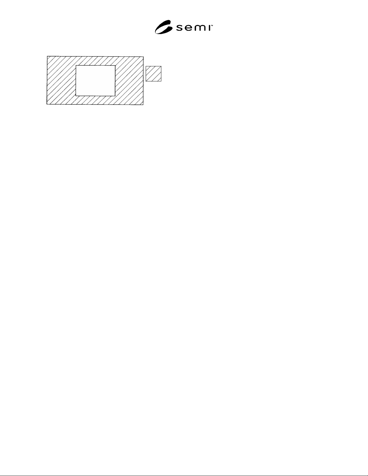
Seal Area
Figure 5
Seal Area
NOTICE: These standards do not purport to address
safety issues, if any, associated with their use. It is the
responsibility of the user of these standards to establish
appropriate safety and health practices and determine
the applicability of regulatory limitations prior to use.
SEMI makes no warranties or representations as to the
suitability of the standards set forth herein for any
particular application. The determination of the
suitability of the standard is solely the responsibility of
the user. Users are cautioned to refer to manufacturer’s
instructions, product labels, product data sheets, and
other relevant literature respecting any materials
mentioned herein. These standards are subject to
change without notice.
The user’s attention is called to the possibility that
compliance with this standard may require use of
copyrighted material or of an invention covered by
patent rights. By publication of this standard, SEMI
takes no position respecting the validity of any patent
rights or copyrights asserted in connection with any
item mentioned in this standard. Users of this standard
are expressly advised that determination of any such
patent rights or copyrights, and the risk of infringement
of such rights, are entirely their own responsibility.
Copyright by SEMI® (Semiconductor Equipment and Materials
International), 3081 Zanker Road, San Jose, CA 95134. Reproduction of
the contents in whole or in part is forbidden without express written
consent of SEMI.