semi合集-English.pdf - 第284页
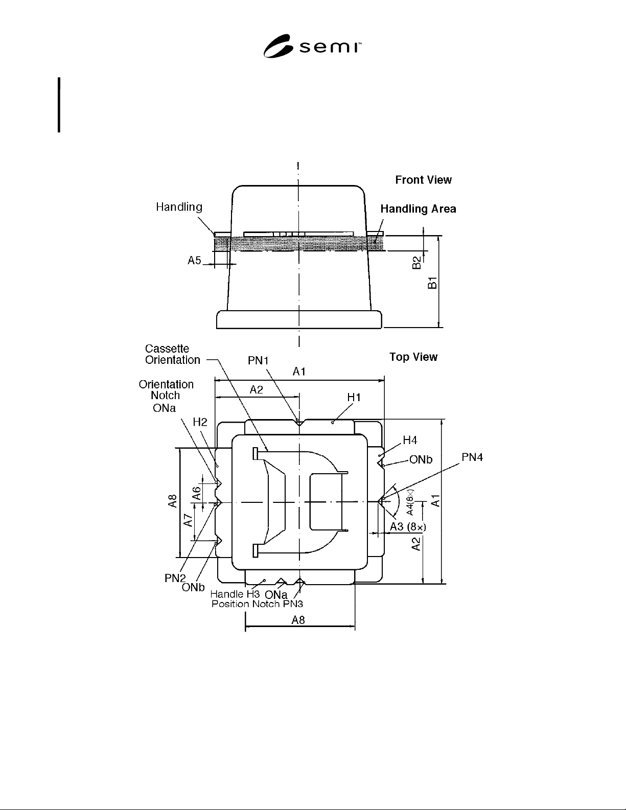
SEMI E47-0301 © SEMI 1995 , 2001 3 Table 1 Handlin g Dimensions for 1 50 mm (6 in.) Pod Handling Dime nsions for 2 00 mm (8 in.) Pod Handle: A 1 215.0 mm ± 0.5 mm (8.464" ± 0.019") 305.0 m m ± 0.5 mm ( 12.008&q…
SEMI E47-0301 © SEMI 1995, 2001 2
6.6 An optional handle to be placed at the top of the pod is specified in SEMI E47.1 (Section 6.9, Figure 12, and
Table 1). If used for 150 mm or 200 mm pods, this “top robotic handling flange” has to meet the required
dimensions as specified in SEMI E47.1 (see Figure 12 of SEMI E47.1). Its center is to be placed above the center of
the cassette in the pod with the two orientation notches at the side where the cassette is accessed to remove wafers.
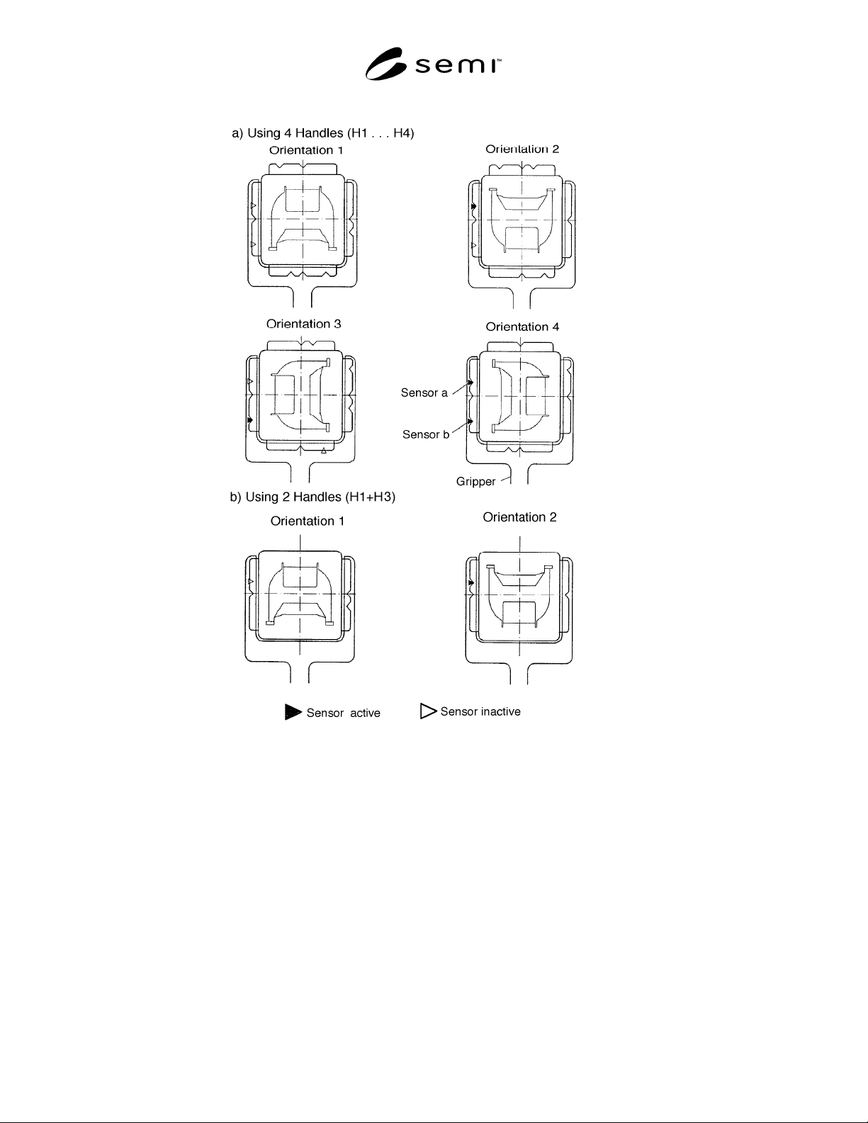
The orientation possibilities of the pod are then the same as described in Section 6.5 above and Table 2.
Figure 1
Pod Handling Terminology and Dimensions
SEMI E47-0301 © SEMI 1995, 20013
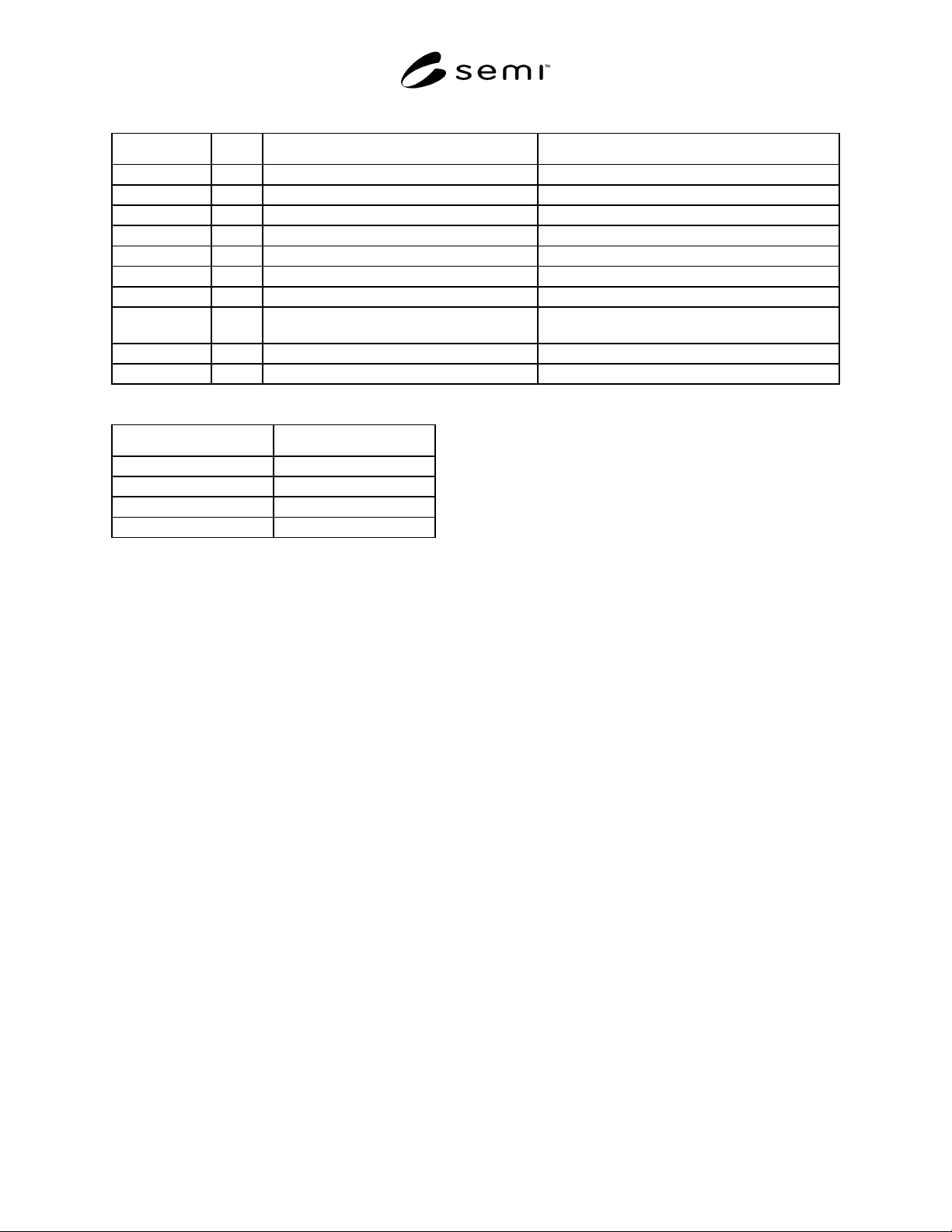
Table 1
Handling Dimensions for 150 mm (6 in.) Pod Handling Dimensions for 200 mm (8 in.) Pod
Handle: A1 215.0 mm ± 0.5 mm (8.464" ± 0.019") 305.0 mm ± 0.5 mm (12.008" ± 0.019")
A2 107.50 mm ± 0.25 mm (4.232" ± 0.01") 152.50 mm ± 0.25 mm (6.004" ± 0.01")
A3 6.0 mm ± 0.2 mm (0.236" ± 0.008") 5.65 mm ± 0.2 mm (0.222" ± 0.008")
A4 90° ± 0.2° 90° ± 0.2° (90° ± 0.2°)
A5 14 mm min. (0.551" min.) 20 mm min. (0.787" min.)
A6 30 mm ± 0.2 mm (1.181" ± 0.008") 30.0 mm ± 0.2 mm (1.181" ± 0.008")
A7 50 mm ± 0.2 mm (1.969" ± 0.008") 50.0 mm ± 0.2 mm (1.969" ± 0.008")
A8 148 mm min., 215 mm max. (A1)
(5.827" min., 8.464" max.)
148 mm min., 305 mm max. (A1)
(5.827" min., 12.008" max.)
Handle Height: B1 158 mm ± 1.0 mm (6.220" ± 0.039") 150.4 mm ± 1.0 mm (5.921" ± 0.039")
Handling Area: B2 30 mm min. (1.181" min.) 30 mm min. (1.181" min.)
Table 2
Orientation # Orientation Notch
1void
2 ON a
3 ON b
4 ON a+b
SEMI E47-0301 © SEMI 1995, 2001 4
Figure 2
Orientation Possibilities
NOTICE: SEMI makes no warranties or representa-tions as to the suitability of the specification set forth herein for
any particular application. The determination of the suitability of the specification is solely the responsibility of the
user. Users are cautioned to refer to manufacturer’s instructions, product labels, product data sheets, and other
relevant literature respecting any materials mentioned herein. These specifications are subject to change without
notice.
The user’s attention is called to the possibility that compliance with this specification may require use of
copyrighted material or of an invention covered by patent rights. By publication of this specification, SEMI takes
no position respecting the validity of any patent rights or copyrights asserted in connection with any item mentioned
in this specification. Users of this specification are expressly advised that determination of any such patent rights or
copyrights, and the risk of infringement of such rights, are entirely their own responsibility.
Copyright by SEMI® (Semiconductor Equipment and Materials
International), 3081 Zanker Road, San Jose, CA 95134. Reproduction o
f
the contents in whole or in part is forbidden without express written
consent of SEMI.